| Sign In | Join Free | My ecer.jp |
|
| Sign In | Join Free | My ecer.jp |
|
| Categories | InP Wafer |
|---|---|
| Brand Name: | PAM-XIAMEN |
| Place of Origin: | China |
| MOQ: | 1-10,000pcs |
| Payment Terms: | T/T |
| Supply Ability: | 10,000 wafers/month |
| Delivery Time: | 5-50 working days |
| Packaging Details: | Packaged in a class 100 clean room environment, in single container, under a nitrogen atmosphere |
| product name: | InP Substrate wafer |
| Wafer Diamter: | 2 inch |
| Conduction Type: | Semi-Insulating |
| Grade: | Test Grade |
| application: | opto-electronic industry |
| keyword: | Indium Phosphide Wafer |
Semi-Insulating , InP Substrate , 2”, Test Grade -Powerway Wafer
PAM-XIAMEN manufactures high purity single crystal Indium Phosphide Wafers for optoelectronics applications. Our standard wafer diameters range from 25.4 mm (1 inch) to 200 mm (6 inches) in size; wafers can be produced in various thicknesses and orientations with polished or unpolished sides and can include dopants. PAM-XIAMEN can produce wide range grades: prime grade, test grade, dummy grade, technical grade, and optical grade. PAM-XIAMEN also offer materials to customer specifications by request, in addition to custom compositions for commercial and research applications and new proprietary technologies.
Semi-Insulating, InP Substrate, 2”, Test Grade
| 2"InP Wafer Specification | ||||
| Item | Specifications | |||
| Conduction Type | SI-type | |||
| Dopant | Iron | |||
| Wafer Diameter | 2" | |||
| Wafer Orientation | 100±0.5° | |||
| Wafer Thickness | 350±25um | |||
| Primary Flat Length | 16±2mm | |||
| Secondary Flat Length | 8±1mm | |||
| Carrier Concentration | ≤3x1016cm-3 | (0.8-6)x1018cm-3 | (0.6-6)x1018cm-3 | N/A |
| Mobility | (3.5-4)x103cm2/V.s | (1.5-3.5)x103cm2/V.s | 50-70cm2/V.s | >1000cm2/V.s |
| Resistivity | N/A | N/A | N/A | >0.5x10⁷Ωcm |
| EPD | <1000cm-2 | <500cm-2 | <1x103cm-2 | <5x103cm-2 |
| TTV | <10um | |||
| BOW | <10um | |||
| WARP | <12um | |||
| Laser Marking | upon request | |||
| Suface Finish | P/E, P/P | |||
| Epi Ready | yes | |||
| Package | Single wafer container or cassette | |||
Wafer Cleaning
Wafer cleaning is an integral part of the wafer industry. The cleaning process involves the removal of particulate and chemical impurities from the semiconductor. It’s imperative during the cleaning process that the substrate is not damaged in any way. Wafer cleaning is ideal for silicon-based materials since it’s the most common element that is used. Some of the benefits of wafer cleaning include:
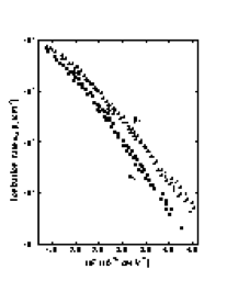 | The dependence of ionization rates for electrons αi and holes βi
versus 1/F, 300 K. (Cook et al. [1982]). |
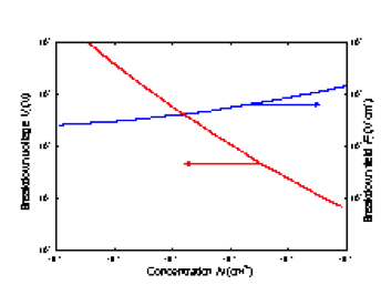 | Breakdown voltage and breakdown field versus doping density for an
abrupt p-n junction, 300 K (Kyuregyan and Yurkov [1989]). |
- for optoelectronic components
- for high-speed electronics.
- for photovoltaics
There is still a vastly under-utilized, yet technically exciting zone in the electromagnetic spectrum between microwaves and infrared, often referred to as “Terahertz”. Electromagnetic waves in this range possess hybrid properties they show high-frequency- and optical characteristics simultaneously. InP based components unlock this spectral range for important new applications.
Are You Looking for an InP substrate?
PAM-XIAMEN is proud to offer indium phosphide substrate for all different kinds of projects. If you are looking for InP wafers, send us enquiry today to learn more about how we can work with you to get you the InP wafers you need for your next project. Our group team is looking forward to providing both quality products and excellent service for you!
|