| Sign In | Join Free | My ecer.jp |
|
| Sign In | Join Free | My ecer.jp |
|
| Categories | InP Wafer |
|---|---|
| Brand Name: | PAM-XIAMEN |
| Place of Origin: | China |
| MOQ: | 1-10,000pcs |
| Payment Terms: | T/T |
| Supply Ability: | 10,000 wafers/month |
| Delivery Time: | 5-50 working days |
| Packaging Details: | Packaged in a class 100 clean room environment, in single container, under a nitrogen atmosphere |
| product name: | single crystal InP Wafer |
| Wafer Diamter: | 2 inch |
| Conduction Type: | P Type |
| Grade: | Prime Grade |
| Wafer Thickness: | 350±25um |
| keyword: | Indium phosphide Wafer |
P Type , VGF InP Wafer With CMP Polished , 2”, Prime Grade , Epi Ready
PAM-XIAMEN provides single crystal InP(Indium phosphide) wafer for micro-electronic ( HBT/ HEMT ) and opto-electronic industry ( LED / DWDM / PIN / VCSELs ) in diameter up to 6 inch. Indium phosphide ( InP ) crystal is formed by two elements , Indium and Phosphide , growth by Liquid Encapsulated Czochralski ( LEC ) method or VGF method . InP wafer is an important semiconductor material which have superior electrical and thermal properties, InP wafer has higher electron mobility, higher frequency, low power consumption , higher thermal conductivity and low noise performance . PAM-XIAMEN can provide epi ready grade InP wafer for your MOCVD & MBE epitaxial application .Please contact our engineer team for more wafer information.
P Type, InP Wafer, 2”, Prime Grade, Epi Ready
| 2"InP Wafer Specification | ||||
| Item | Specifications | |||
| Conduction Type | P-type | |||
| Dopant | Zinc | |||
| Wafer Diameter | 2" | |||
| Wafer Orientation | 100±0.5° | |||
| Wafer Thickness | 350±25um | |||
| Primary Flat Length | 16±2mm | |||
| Secondary Flat Length | 8±1mm | |||
| Carrier Concentration | ≤3x1016cm-3 | (0.8-6)x1018cm-3 | (0.6-6)x1018cm-3 | N/A |
| Mobility | (3.5-4)x103cm2/V.s | (1.5-3.5)x103cm2/V.s | 50-70cm2/V.s | >1000cm2/V.s |
| Resistivity | N/A | N/A | N/A | >0.5x10⁷Ω.cm |
| EPD | <1000cm-2 | <1x103cm-2 | <1x103cm-2 | <5x103cm-2 |
| TTV | <10um | |||
| BOW | <10um | |||
| WARP | <12um | |||
| Laser Marking | upon request | |||
| Suface Finish | P/E, P/P | |||
| Epi Ready | yes | |||
| Package | Single wafer container or cassette | |||
Indium Phosphide Facts
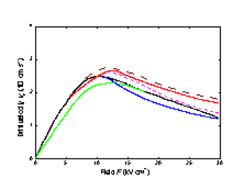 | Field dependences of the electron drift velocity in InP, 300 K. Solid curve are theoretical calculation. Dashed and dotted curve are measured data. (Maloney and Frey [1977]) and (Gonzalez Sanchez et al. [1992]). |
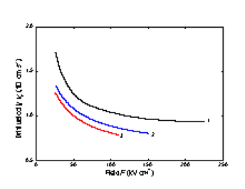 | The field dependences of the electron drift velocity for high
electric fields. T(K): 1. 95; 2. 300; 3. 400. (Windhorn et al. [1983]). |
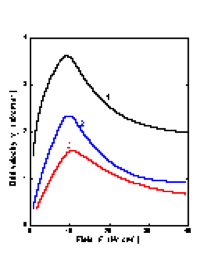 | Field dependences of the electron drift velocity at different
temperatures. Curve 1 -77 K (Gonzalez Sanchez et al. [1992]). Curve 2 - 300 K, Curve 3 - 500 K (Fawcett and Hill [1975]). |
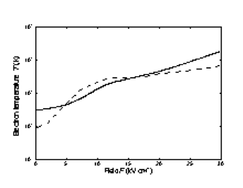 | Electron temperature versus electric field for 77 K and 300 K. (Maloney and Frey [1977]) |
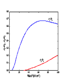 | Fraction of electrons in L and X valleys nL/no and nX/no as a
function of electric field, 300 K. (Borodovskii and Osadchii [1987]). |
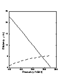 | Frequency dependence of the efficiency η at first (solid line) and
at the second (dashed line) harmonic in LSA mode. Monte Carlo simulation. F = Fo + F1·sin(2π·ft) + F2·[sin(4π·ft)+3π/2], Fo=F1=35 kV cm-1, F2=10.5 kV cm-1 (Borodovskii and Osadchii [1987]). |
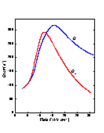 | Longitudinal (D || F) and transverse (D ⊥ F) electron diffusion
coefficients at 300 K. Ensemble Monte Carlo simulation. (Aishima and Fukushima [1983]). |
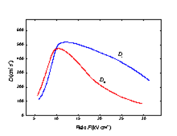 | Longitudinal (D || F) and transverse (D ⊥ F) electron diffusion
coefficients at 77K. Ensemble Monte Carlo simulation. (Aishima and Fukushima [1983]). |
Widely discussed in the LiDAR arena is the wavelength of the signal. While some players have opted for 830-to-940-nm wavelengths to take advantage of available optical components, companies (including Blackmore, Neptec, Aeye, and Luminar) are increasingly turning to longer wavelengths in the also-well-served 1550-nm wavelength band, as those wavelengths allow laser powers roughly 100 times higher to be employed without compromising public safety. Lasers with emission wavelengths longer than ≈ 1.4 μm are often called “eye-safe” because light in that wavelength range is strongly absorbed in the eye's cornea, lens and vitreous body and therefore cannot damage the sensitive retina).
• LiDAR-based sensor technology can provide a high level of object identification and classification with three-dimensional (3D) imaging techniques.
• The automotive industry will adopt a chip-based, low cost solid state LiDAR sensor technology instead of large, expensive, mechanical LiDAR systems in the future.
• For the most advanced chip-based LiDAR systems, InP will play an important role and will enable autonomous driving. (Report: Blistering Growth for Automotive Lidar, Stewart Wills). The longer eye safe wavelength is also more appropriate dealing with real world conditions like dust, fog and rain.
Are You Looking for an InP substrate?
PAM-XIAMEN is proud to offer indium phosphide substrate for all different kinds of projects. If you are looking for InP wafers, send us enquiry today to learn more about how we can work with you to get you the InP wafers you need for your next project. Our group team is looking forward to providing both quality products and excellent service for you!

|
