| Sign In | Join Free | My ecer.jp |
|
| Sign In | Join Free | My ecer.jp |
|
| Categories | InP Wafer |
|---|---|
| Brand Name: | PAM-XIAMEN |
| Place of Origin: | China |
| MOQ: | 1-10,000pcs |
| Payment Terms: | T/T |
| Supply Ability: | 10,000 wafers/month |
| Delivery Time: | 5-50 working days |
| Packaging Details: | Packaged in a class 100 clean room environment, in single container, under a nitrogen atmosphere |
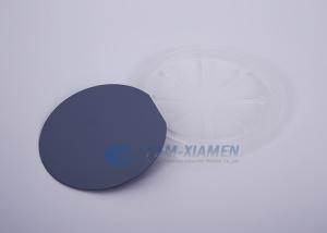
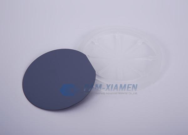
| product name: | Semi-Insulating InP wafer |
| Wafer Diamter: | 2 inch |
| Epi Ready: | yes |
| Grade: | Prime Grade |
| application: | opto-electronic industry |
| keyword: | Indium Phosphide Wafer |
Semi-Insulating, InP Substrate, 2”, Prime Grade, Epi Ready
PAM-XIAMEN offers InP wafer – Indium Phosphide which are grown by
LEC(Liquid Encapsulated Czochralski) or VGF(Vertical Gradient
Freeze) as epi-ready or mechanical grade with n type, p type or
semi-insulating in different orientation(111)or(100).
Indium phosphide (InP) is a binary semiconductor composed of indium
and phosphorus. It has a face-centered cubic (“zinc blende”)
crystal structure, identical to that of GaAs and most of the III-V
semiconductors.Indium phosphide can be prepared from the reaction
of white phosphorus and indium iodide[clarification needed] at 400
°C.,[5] also by direct combination of the purified elements at high
temperature and pressure, or by thermal decomposition of a mixture
of a trialkyl indium compound and phosphide. InP is used in
high-power and high-frequency electronics[citation needed] because
of its superior electron velocity with respect to the more common
semiconductors silicon and gallium arsenide.
Semi-Insulating, InP Substrate, 2”, Prime Grade, Epi Ready
| 2"InP Wafer Specification | ||||
| Item | Specifications | |||
| Conduction Type | SI-type | |||
| Dopant | Iron | |||
| Wafer Diameter | 2" | |||
| Wafer Orientation | 100±0.5° | |||
| Wafer Thickness | 350±25um | |||
| Primary Flat Length | 16±2mm | |||
| Secondary Flat Length | 8±1mm | |||
| Carrier Concentration | ≤3x1016cm-3 | (0.8-6)x1018cm-3 | (0.6-6)x1018cm-3 | N/A |
| Mobility | (3.5-4)x103cm2/V.s | (1.5-3.5)x103cm2/V.s | 50-70cm2/V.s | >1000cm2/V.s |
| Resistivity | N/A | N/A | N/A | >0.5x10⁷Ωcm |
| EPD | <1000cm-2 | <500cm-2 | <1x103cm-2 | <5x103cm-2 |
| TTV | <10um | |||
| BOW | <10um | |||
| WARP | <12um | |||
| Laser Marking | upon request | |||
| Suface Finish | P/E, P/P | |||
| Epi Ready | yes | |||
| Package | Single wafer container or cassette | |||
Most test wafers are wafers which have fallen out of prime specifications. Test wafers may be used to run marathons, test equipment and for high-end R & D. They are often a cost-effective alternative to prime wafers.
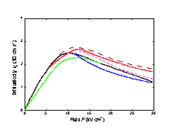 | Field dependences of the electron drift velocity in InP, 300 K. Solid curve are theoretical calculation. Dashed and dotted curve are measured data. (Maloney and Frey [1977]) and (Gonzalez Sanchez et al. [1992]). |
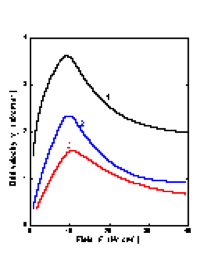
 | The field dependences of the electron drift velocity for high
electric fields. T(K): 1. 95; 2. 300; 3. 400. (Windhorn et al. [1983]). |
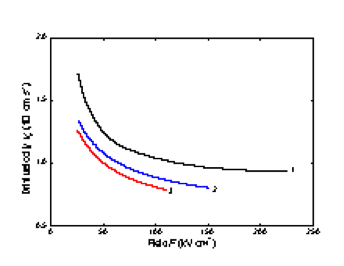
 | Field dependences of the electron drift velocity at different
temperatures. Curve 1 -77 K (Gonzalez Sanchez et al. [1992]). Curve 2 - 300 K, Curve 3 - 500 K (Fawcett and Hill [1975]). |
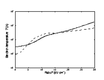 | Electron temperature versus electric field for 77 K and 300 K. (Maloney and Frey [1977]) |
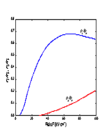 | Fraction of electrons in L and X valleys nL/no and nX/no as a
function of electric field, 300 K. (Borodovskii and Osadchii [1987]). |
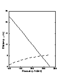 | Frequency dependence of the efficiency η at first (solid line) and
at the second (dashed line) harmonic in LSA mode. Monte Carlo simulation. F = Fo + F1·sin(2π·ft) + F2·[sin(4π·ft)+3π/2], Fo=F1=35 kV cm-1, F2=10.5 kV cm-1 (Borodovskii and Osadchii [1987]). |
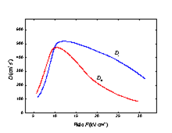
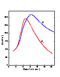 | Longitudinal (D || F) and transverse (D ⊥ F) electron diffusion
coefficients at 300 K. Ensemble Monte Carlo simulation. (Aishima and Fukushima [1983]). |
 | Longitudinal (D || F) and transverse (D ⊥ F) electron diffusion
coefficients at 77K. Ensemble Monte Carlo simulation. (Aishima and Fukushima [1983]). |
InP is used in high-power and high-frequency electronics[citation
needed] because of its superior electron velocity with respect to
the more common semiconductors silicon and gallium arsenide.
It was used with indium gallium arsenide to make a record breaking
pseudomorphic heterojunction bipolar transistor that could operate
at 604 GHz.
It also has a direct bandgap, making it useful for optoelectronics
devices like laser diodes. The company Infinera uses indium
phosphide as its major technological material for manufacturing
photonic integrated circuits for the optical telecommunications
industry, to enable wavelength-division multiplexing applications.
InP is also used as a substrate for epitaxial indium gallium
arsenide based opto-electronic devices.
PAM-XIAMEN is your go-to place for everything wafers, including InP wafers, as we have been doing it for almost 30 years! Enquire us today to learn more about the wafers that we offer and how we can help you with your next project. Our group team is looking forward to providing both quality products and excellent service for you!
|