| Sign In | Join Free | My ecer.jp |
|
| Sign In | Join Free | My ecer.jp |
|
| Categories | GaAs Wafer |
|---|---|
| Brand Name: | zmsh |
| Model Number: | GaAs-4inch |
| Certification: | no |
| Place of Origin: | china |
| MOQ: | 5pcs |
| Price: | by case |
| Supply Ability: | 1000pcs/month |
| Delivery Time: | 1-4weeks |
| Packaging Details: | 25pcs casstle in 100-grade cleaning room |
| material: | GaAs single crystal substrates |
| industry: | semicondutor wafer |
| application: | semiconductor substrate, led chip, optical glass window,device substrates |
| method: | VFG |
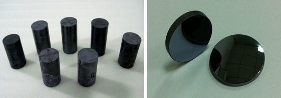
| size: | 2-6inch commen |
| Company Info. |
| SHANGHAI FAMOUS TRADE CO.,LTD |
| Verified Supplier |
| View Contact Details |
| Product List |
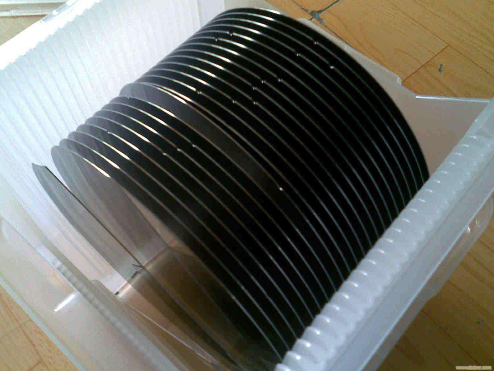
4inch GaAs substrates, GaAs wafer for led,Gallium Arsenide crystal Wafers,Si/Zn Dopant GaAs wafer
(A compound of the elements gallium and arsenic. It is a III-V direct bandgap semiconductor with a zinc blende crystal structure)
--------------------------------------------------------------------------------------------------------------
About GaAs crystal
| Product Name: | Gallium arsenide (GaAs) crystal substrate | ||||||||||||
| Technical parameters: |
| ||||||||||||
| Specifications: | General orientation: <100>: <110>: <111>: Standard Size: Ø3 "x 0.5mm; Ø2" x 0.5mm ; Ø4 "x 0.5mm ; Note: according to customers' requirements and size of the corresponding direction. |
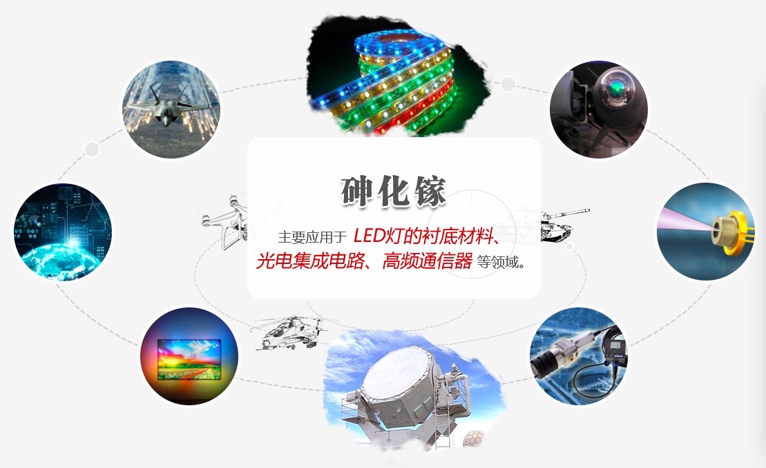
Application:
1. Mainly used in electronics, low temperature alloys, Gallium Arsenide.
2. The primary chemical compound of gallium in electronics, is used in microwave circuits, high-speed switching circuits, and infrared circuits.
3. Gallium Nitride and Indium Gallium Nitride, for semiconductor uses, produce blue and violet light-emitting diodes (LEDs) and diode lasers.
Specification
GaAs Wafers for LED Applications
| Item | Specifications | Remarks |
| Conduction Type | SC/n-type | SC/p-type with Zn dope Available |
| Growth Method | VGF | |
| Dopant | Silicon | Zn available |
| Wafer Diamter | 2, 3 & 4 inch | Ingot or as-cut availalbe |
| Crystal Orientation | (100)20/60/150 off (110) | Other misorientation available |
| OF | EJ or US | |
| Carrier Concentration | (0.4~2.5)E18/cm3 | |
| Resistivity at RT | (1.5~9)E-3 Ohm.cm | |
| Mobility | 1500~3000cm2/V.sec | |
| Etch Pit Density | <5000/cm2 | |
| Laser Marking | upon request | |
| Surface Finish | P/E or P/P | |
| Thickness | 220~450um | |
| Epitaxy Ready | Yes | |
| Package | Single wafer container or cassette | |
(GaAs)Gallium Arsenide Wafers for LD Applications
| Item | Specifications | Remarks |
| Conduction Type | SC/n-type | |
| Growth Method | VGF | |
| Dopant | Silicon | |
| Wafer Diamter | 2, 3 & 4 inch | Ingot or as-cut available |
| Crystal Orientation | (100)20/60/150 off (110) | Other misorientation available |
| OF | EJ or US | |
| Carrier Concentration | (0.4~2.5)E18/cm3 | |
| Resistivity at RT | (1.5~9)E-3 Ohm.cm | |
| Mobility | 1500~3000 cm2/V.sec | |
| Etch Pit Density | <500/cm2 | |
| Laser Marking | upon request | |
| Surface Finish | P/E or P/P | |
| Thickness | 220~350um | |
| Epitaxy Ready | Yes | |
| Package | Single wafer container or cassette | |
(GaAs)Gallium Arsenide Wafers,Semi-insulating for Microelectronics Applications
| Item | Specifications | Remarks |
| Conduction Type | Insulating | |
| Growth Method | VGF | |
| Dopant | Undoped | |
| Wafer Diamter | 2, 3 & 4 inch | Ingot available |
| Crystal Orientation | (100)+/- 0.50 | |
| OF | EJ, US or notch | |
| Carrier Concentration | n/a | |
| Resistivity at RT | >1E7 Ohm.cm | |
| Mobility | >5000 cm2/V.sec | |
| Etch Pit Density | <8000 /cm2 | |
| Laser Marking | upon request | |
| Surface Finish | P/P | |
| Thickness | 350~675um | |
| Epitaxy Ready | Yes | |
| Package | Single wafer container or cassette | |
FAQ –
Q: What you can supply logistics and cost?
(1) We accept DHL, Fedex, TNT, UPS, EMS, SF and etc.
(2) If you have your own express number, it's great.
If not, we could assist you to deliver. Freight=USD25.0(the first
weight) + USD12.0/kg
Q: What's the delivery time?
(1) For the standard products such as ball lens, powell lens and
collimator lens:
For inventory: the delivery is 5 workdays after order.
For customized products: the delivery is 2 or 3 workweeks after
order.
(2) For the off-standard products, the delivery is 2 or 6 workweeks
after you place the order.
Q: How to pay?
T/T, Paypal, West Union, MoneyGram, Secure payment and Trade
Assurance on and etc..
Q: What's the MOQ?
(1) For inventory, the MOQ is 5pcs.
(2) For customized products, the MOQ is 5pcs-20pcs.
It depends on quantity and technics
Q: Do you have inspection report for material?
We can supply detail report for our products.
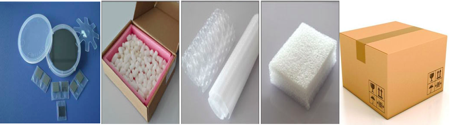
Packaging – Logistcs
Worldhawk concerns each details of the package , cleaning,
anti-static , shock treatment . According to the quantity and shape
of the product , we will take a different packaging process!
|
