| Sign In | Join Free | My ecer.jp |
|
| Sign In | Join Free | My ecer.jp |
|
| Categories | GaAs Wafer |
|---|---|
| Brand Name: | zmsh |
| Model Number: | ZnO |
| Certification: | no |
| Place of Origin: | china |
| MOQ: | 5cs |
| Price: | by case |
| Supply Ability: | 500pcs/month |
| Delivery Time: | 1-4weeks |
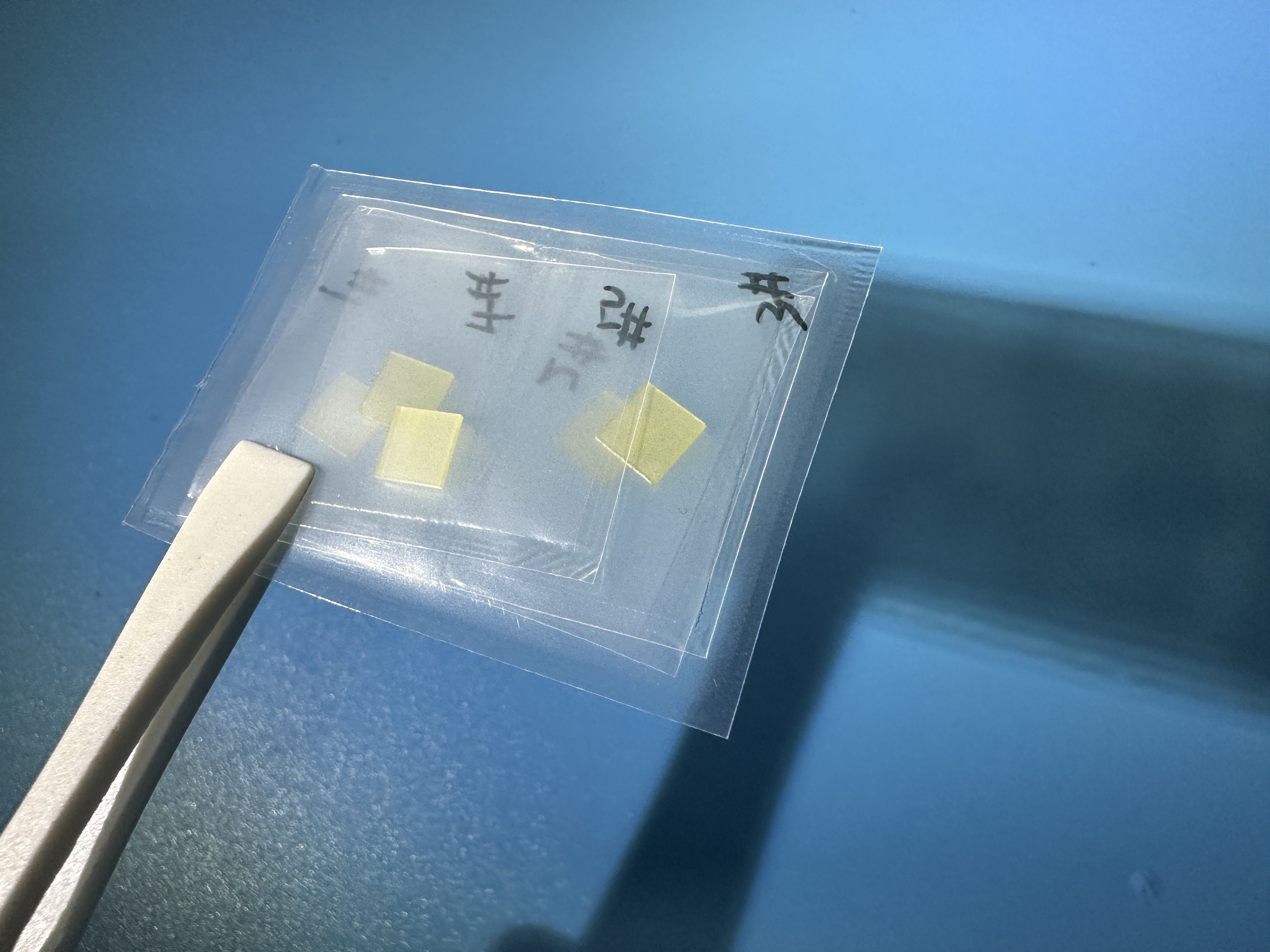
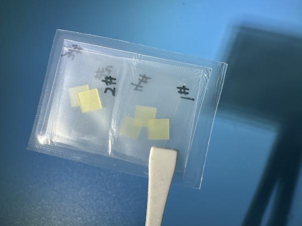
| Packaging Details: | PET film in 100-grade cleaning room |
| material: | ZnO single crystal substrates |
| industry: | semicondutor wafer |
| application: | semiconductor substrate, led chip, optical glass window,device substrates |
| method: | VFG |
| size: | 5X5mm |
| Thickness: | 0.5mm |
| Company Info. |
| SHANGHAI FAMOUS TRADE CO.,LTD |
| Verified Supplier |
| View Contact Details |
| Product List |
ZnO substrates,5X5mm small square Zinc oxide wafer,5x5mm ZnO substrates in different orientations, ZnO single crystal.
--------------------------------------------------------------------------------------------------------------
Zinc Oxide (ZnO) can be grown as a single crystal semiconductor with very interesting properties.
The bandgap is in the 3.4 eV range which makes it attractive for many of the blue and violet applications
in opto-electronics as well as UV devices. It is available in bulks, in wafers of up to 2 inches,
which gives it a major advantage over Gallium Nitride and other
group III Nitrides.
ZnO also has the potential to become the substrate material of
choice for GaN. Like GaN it has a wurtzite structure, with lattice
constants closely matched to GaN (a=3.249, c=5.205). ZnO is exactly
lattice matched to InGaN with a 22% In content. Perhaps most importantly it is a soft compliant material
that is believed to probably and may take up the lattice stress in preference to the growing GaN layer.
It suffers from the drawback that it dissociates in ammonia at temperatures above 600°C. With its wide bandgap, Zinc Oxide could prove very useful in optical applications as well as many high speed electronics.
ZnO may also be used as a substrate for epitaxial growth.
Application:
Zinc oxide (ZnO) crystal substrateProduct Description:Zinc oxide (ZnO) crystal substrate is widely used in
GaN (blue LED) epitaxial substrate, broad band connecting devices and other fields.Technical parameters

General Properties
| Purity wt% | > 99.99 |
| Impurity: wt% | Mg: <.0005 Al: < .0030 Si: 0.0030 Ti: .0010 Cu: < .0030 |
| Fe: < 0.005 Ca: <.0005 Ag: < .0002 | |
| Crystal Structure | Hexagonal: a= 3.252 å , c = 5.207 å |
| Growth Method | Hydrothermal |
| Hardness | 4 moh scale |
| Density | 5.7 g/cm3 |
| Melt Point | 1975 oC |
| Specific heat | 0.125 cal/gm |
| Thermoelectric Constant | 1200 mV /oK @ 300 oC |
| Thermal conductivity | 0.006 cal/cm/ oK |
| Thermal expansion | 2.90 x 10⁻⁶/oK |
| Transmission range | 0.4 - 0.6 m > 50% at 2 mm |
| Dislocation Density | <0001> plane <100 / cm2 |
Specifications for wafer
| Orientation | <11-20>± 0.5o or custom orientation |
| Polished surface | EPI polished on one side ,Ra < 5 Å |
| Standard Size | 5 x 5 mm |
| Thickness | 0.5 mm |

FAQ –
Q: What you can supply logistics and cost?
(1) We accept DHL, Fedex, TNT, UPS, EMS, SF and etc.
(2) If you have your own express number, it's great.
If not, we could assist you to deliver. Freight=USD25.0(the first
weight) + USD12.0/kg
Q: What's the delivery time?
(1) For the standard products such as ball lens, powell lens and
collimator lens:
For inventory: the delivery is 5 workdays after order.
For customized products: the delivery is 2 or 3 workweeks after
order.
(2) For the off-standard products, the delivery is 2 or 6 workweeks
after you place the order.
Q: How to pay?
100%T/T, Paypal, West Union, MoneyGram, Secure payment and Trade
Assurance on and etc..
Q: What's the MOQ?
(1) For inventory, the MOQ is 5pcs.
(2) For customized products, the MOQ is 5pcs-20pcs.
It depends on quantity and technics
Q: Do you have inspection report for material?
We can supply detail report for our products.
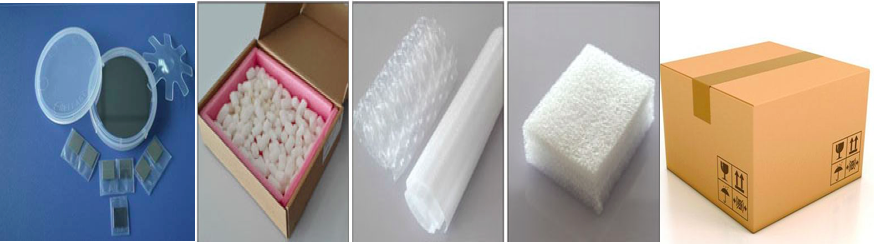
Packaging – Logistcs
Worldhawk concerns each details of the package , cleaning,
anti-static , shock treatment .
According to the quantity and shape of the product , we will take a different packaging process!
|
