| Sign In | Join Free | My ecer.jp |
|
| Sign In | Join Free | My ecer.jp |
|
| Categories | GaAs Wafer |
|---|---|
| Brand Name: | ZMSH |
| Model Number: | GaP Wafers |
| Certification: | ROHS |
| Place of Origin: | China |
| MOQ: | 25pcs |
| Price: | Negotiation |
| Payment Terms: | T/T |
| Delivery Time: | In 30 days |
| Packaging Details: | Customized Box |
| Material: | GaP Wafers |
| Diameter: | 6'' 8'' |
| Thickness: | 200um 350um |
| Orientation: | (110)A 0°+0.2 |
| Growth Method: | LPE |
| Refractive index: | 3.19 |
| TTV: | 8um |
| Warp: | 8um |
| Bow: | 8um |
| Company Info. |
| SHANGHAI FAMOUS TRADE CO.,LTD |
| Verified Supplier |
| View Contact Details |
| Product List |
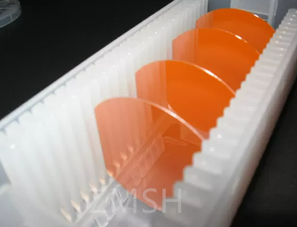
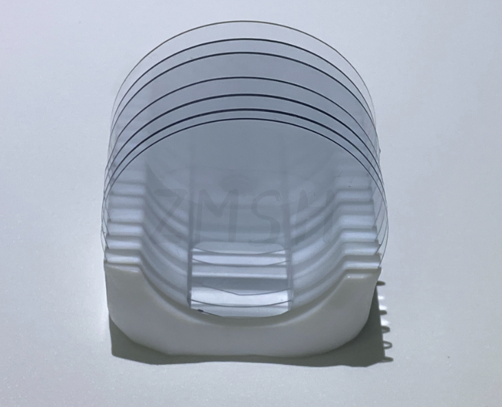
Transparent Orange Undopped GaP Wafers P Type N Type 200um 350um 5G Light Emitting
Description:
Gallium Phosphide GaP, an important semiconductor of unique electrical properties as other III-V compound materials, crystallizes in the thermodynamically stable cubic ZB structure, is an orange-yellow semitransparent crystal material with an indirect band gap of 2.26 eV (300K), which is synthesized from 6N 7N high purity gallium and phosphorus, and grown into single crystal by Liquid Encapsulated Czochralski (LEC) technique. Gallium Phosphide crystal is doped sulfur or tellurium to obtain n-type semiconductor, and zinc doped as p-type conductivity for further fabricating into desired wafer, which has applications in optical system, electronic and other optoelectronics devices. Single Crystal GaP wafer can be prepared Epi-Ready for your LPE, MOCVD and MBE epitaxial application. High quality single crystal Gallium phosphide GaP wafer p-type, n-type or undoped conductivity at Western Minmetals (SC) Corporation can be offered in size of 2″and 3” (50mm, 75mm diameter) , orientation <100>,<111> with surface finish of as-cut, polished or epi-ready process.
Features:
Wide bandgap suitable for emitting specific wavelengths of
light.GaP Wafer Excellent optical properties enabling LED
production in various colors.
High efficiency in generating red, yellow, and green lights for
LEDs.Superior light absorption ability at specific wavelengths.
Good electrical conductivity facilitating high-frequency electronic
devices. GaP Wafer Appropriate thermal stability for reliable
performance. Chemical stability suitable for semiconductor
manufacturing processes. GaP Wafer Favorable lattice parameters for
epitaxial growth of additional layers. Capability to serve as a
substrate for semiconductor deposition. GaP Wafer Robust material
with high thermal conductivity. Excellent optoelectronic
capabilities for photodetectors. Versatility in designing optical
devices for specific wavelength ranges
Technical Parameters:
| Items | Parameters |
| Colour | Transparent Orange Red |
| Diameter | 6’’ 8’’ |
| Thickness | 200um 350um |
| Type | P-type N-type |
| Density | 4.250 g/cm3 |
| Melting point | 1478 °C |
| Growth method | LPE |
| Solubility | soluble |
| Orientation | (110)A 0°+0.2 |
| Refractive index | 3.19 |
| Warp | 8um |
| Bow | 8um |
| TTV | 8um |
| Grade | P R A |
| Origin | China |
| Application | 5G |
Applications:
Gallium phosphide single crystal through slicing, epitaxy and other processes can be made into solid light emitting devices, its life is long, is semi-permanent. This device has developed rapidly and is widely used in instruments, computers and electronic watches, etc., for digital display or indicator light, it can emit red or green light, etc. (the luminous wavelength varies with doping). Early light-emitting devices made of gallium arsenide needed a current of 100 milliamps to emit 20 millilumens per word. The same light-emitting device made of gallium phosphide requires only 10 milliamps of current to emit 20 millilumens. The efficiency of gallium phosphide light-emitting tube made by two-layer epitaxy method is 4-5%. Wingloff believes that the main factor affecting the efficiency of gallium phosphates light-emitting devices is the dislocation density in the crystal, and the luminous efficiency is low when the dislocation density is high.

Other product:
FAQ:
Q: What is the Brand Name of the GaP Wafers?
A: The Brand Name of the GaP Wafers is ZMSH.
Q: What is the Certification of the GaP Wafers?
A: The Certification of the GaP Wafers is ROHS.
Q: Where is the Place of Origin of the GaP Wafers?
A: The Place of Origin of the GaP Wafers is CHINA.
Q: What is the MOQ of the GaP Wafers at one time?
A: The MOQ of the GaP Wafers is 25pcs at one time.

|
