| Sign In | Join Free | My ecer.jp |
|
| Sign In | Join Free | My ecer.jp |
|
| Categories | Gallium Nitride Wafer |
|---|---|
| Brand Name: | ZMSH |
| Model Number: | GaN-on-Si Wafer |
| Place of Origin: | China |
| Payment Terms: | T/T |
| Delivery Time: | 2-4weeks |
| Polished: | DSP SSP |
| Doping Concentration: | Concentration Of The Doping Element 1×10^16 - 1×10^18 Cm^-3 |
| Defect Density: | ≤500 Cm^-2 |
| Storage Conditions: | Storage Environment For The Wafer Temperature 20-25°C, Humidity ≤60% |
| Mobility: | 1200~2000 |
| Thickness: | 350 + 10um |
| Flatness: | Flatness Of The Wafer Surface ≤0.5 μm |
| Diameter: | 2-8inch |
| Company Info. |
| SHANGHAI FAMOUS TRADE CO.,LTD |
| Verified Supplier |
| View Contact Details |
| Product List |
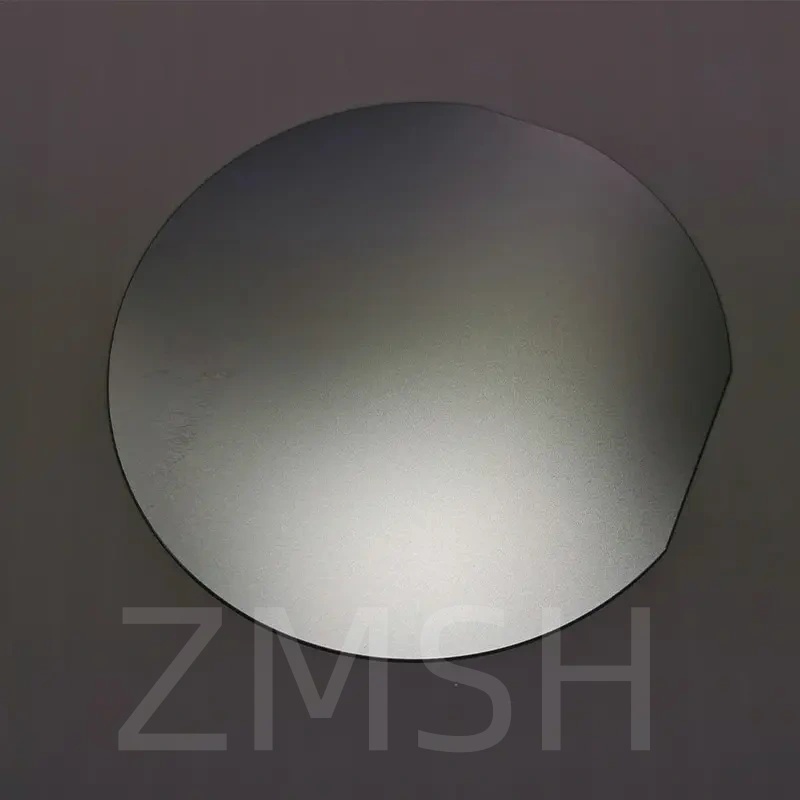
8inch GaN-on-Si Epitaxy Wafer 110 111 110 N-type P-type Customization Semiconductor RF LED
The 8-inch-diameter GaN-on-Si MMIC and Si CMOS wafers (above, left) are 3D integrated at the wafer scale. The two wafers are bonded face-to-face using a low-temperature oxide-oxide bonding technique. The Si substrate of the silicon-on-insulator wafer is completely removed by grinding and selective wet etch to stop at the buried oxide (BOX). Vias to the back of CMOS and to the top of GaN circuits are etched separately and interconnected with a top metal. The vertical integration minimizes the chip size and reduces the interconnect distance to lower the loss and delay. In addition to the oxide-oxide bond approach, work is underway to expand the capabilities of the 3D integration approach by using hybrid bond interconnects, which would allow direct electrical connections between the two wafers without separate vias to the GaN and CMOS circuits.
High uniformity
Low leakage current
Higher operating temperatures
Excellent 2DEG characteristic
High breakdown voltage (600V-1200V)
Lower ON-resistance
Higher switching frequencies
Higher operating frequencies (up to 18GHz)
CMOS-compatible process for GaN-on-Si MMICs
Use of 200-mm-diameter Si substrate and CMOS tools reduces cost and increases yield
Wafer-scale 3D integration of GaN MMICs with CMOS to enhance functionalities with improved size, weight, and power benefits
The Form of GaN-on-Si Wafers:
| ITEM | Gallium Nitride on Silicon wafer, GaN on Silicon wafer |
| GaN thin film | 0.5μm ± 0.1 μm |
| GaN orientation | C-plane (0001) |
| Ga-face | <1nm, As-grown, EPI-ready |
| N-face | P-type/B-doped |
| Polarity | Ga-face |
| Conductivity type | Undoped/N-type |
| Macro defect density | <5/cm^2 |
| Silicon wafer substrate | |
| Orientation | <100> |
| Conductivity type | N-type/P-doped or P-type/B-doped |
| Dimension: | 10 x 10 x 0.5mm 2inch 4inch 6inch 8inch |
| Resistivity | 1-5 ohm-cm, 0-10 ohm-cm, <0.005 ohm-cm or others |
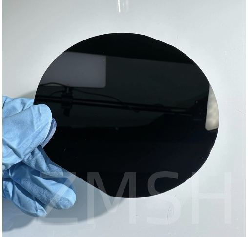
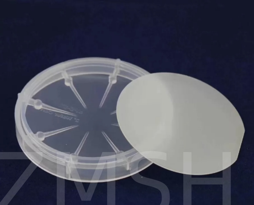
The Physical Photo of GaN-on-Si Wafers:
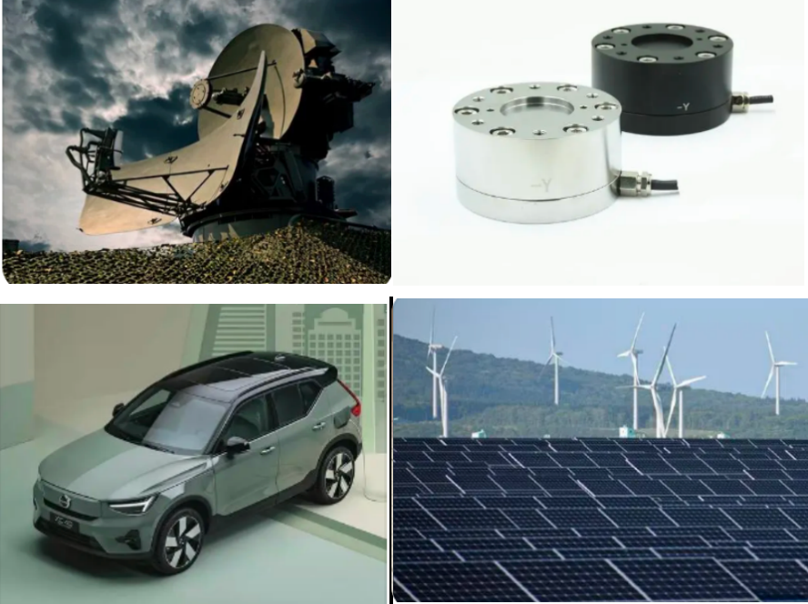
Application of GaN-on-Si Wafers:
1. Lighting: GaN-on-Si substrates are used in the manufacturing of
high-brightness light-emitting diodes (LEDs) for various
applications such as general lighting, automotive lighting,
backlighting for displays, and more. GaN LEDs are energy-efficient
and long-lasting.
2. Power Electronics: GaN-on-Si substrates are utilized in the
production of power electronic devices like high-electron-mobility
transistors (HEMTs) and Schottky diodes. These devices are employed
in power supplies, inverters, and converters due to their high
efficiency and fast switching speeds.
3. Wireless Communication: GaN-on-Si substrates are used in the
development of high-frequency and high-power RF devices for
wireless communication systems like radar systems, satellite
communication, and base stations. GaN RF devices offer high power
density and efficiency.
4. Automotive: GaN-on-Si substrates are increasingly being used in
the automotive industry for applications such as onboard chargers,
DC-DC converters, and motor drives due to their high power density,
efficiency, and reliability.
5. Solar Power: GaN-on-Si substrates can be employed in the
production of solar cells, where their high efficiency and
resistance to radiation damage can be advantageous for space
applications and concentrated photovoltaics.
6. Sensors: GaN-on-Si substrates can be utilized in the development
of sensors for various applications, including gas sensors, UV
sensors, and pressure sensors, due to their high sensitivity and
stability.
7. Biomedical: GaN-on-Si substrates have potential applications in
biomedical devices for sensing, imaging, and therapy due to their
biocompatibility, stability, and ability to operate in harsh
environments.
8. Consumer Electronics: GaN-on-Si substrates are used in consumer
electronics for various applications like wireless charging, power
adapters, and high-frequency circuits due to their high efficiency
and compact size.
Application Picture of GaN-on-Si Wafers:
FAQ:
1.Q:What is the process of GaN on silicon?
A: 3D stacking technology. Upon separation, the silicon donor wafer
cleaves along a weakened crystal plane and thereby leaves a thin
layer of silicon channel material on the GaN wafer. This silicon
channel is then processed into silicon PMOS transistors on the GaN
wafer.
2.Q:What are the advantages of gallium nitride over silicon?
A:Gallium nitride (GaN) is a very hard, mechanically stable, binary
III/V direct bandgap semiconductor. With higher breakdown strength,
faster switching speed, higher thermal conductivity and lower
on-resistance, power devices based on GaN significantly outperform
silicon-based devices.
Product Recommend:
2.2inch 4inch free-standing GaN Gallium Nitride Wafer

|
