| Sign In | Join Free | My ecer.jp |
|
| Sign In | Join Free | My ecer.jp |
|
| Categories | Gallium Nitride Wafer |
|---|---|
| Brand Name: | zmkj |
| Model Number: | GaN-FS-C-U-C50-SSP |
| Place of Origin: | CHINA |
| MOQ: | 1pcs |
| Price: | 1000~3000usd/pc |
| Payment Terms: | T/T |
| Supply Ability: | 50pcs per month |
| Delivery Time: | 1-5weeks |
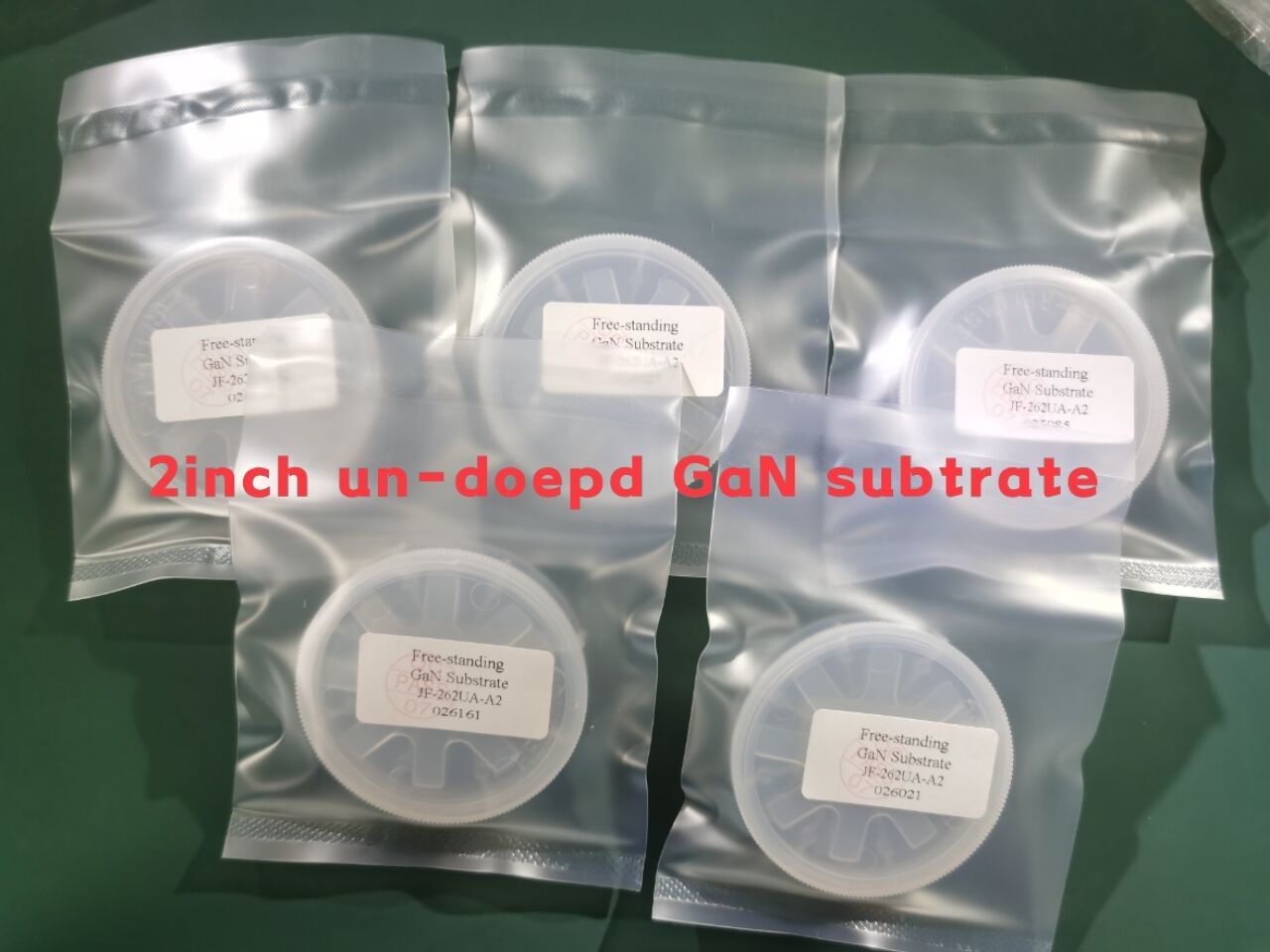
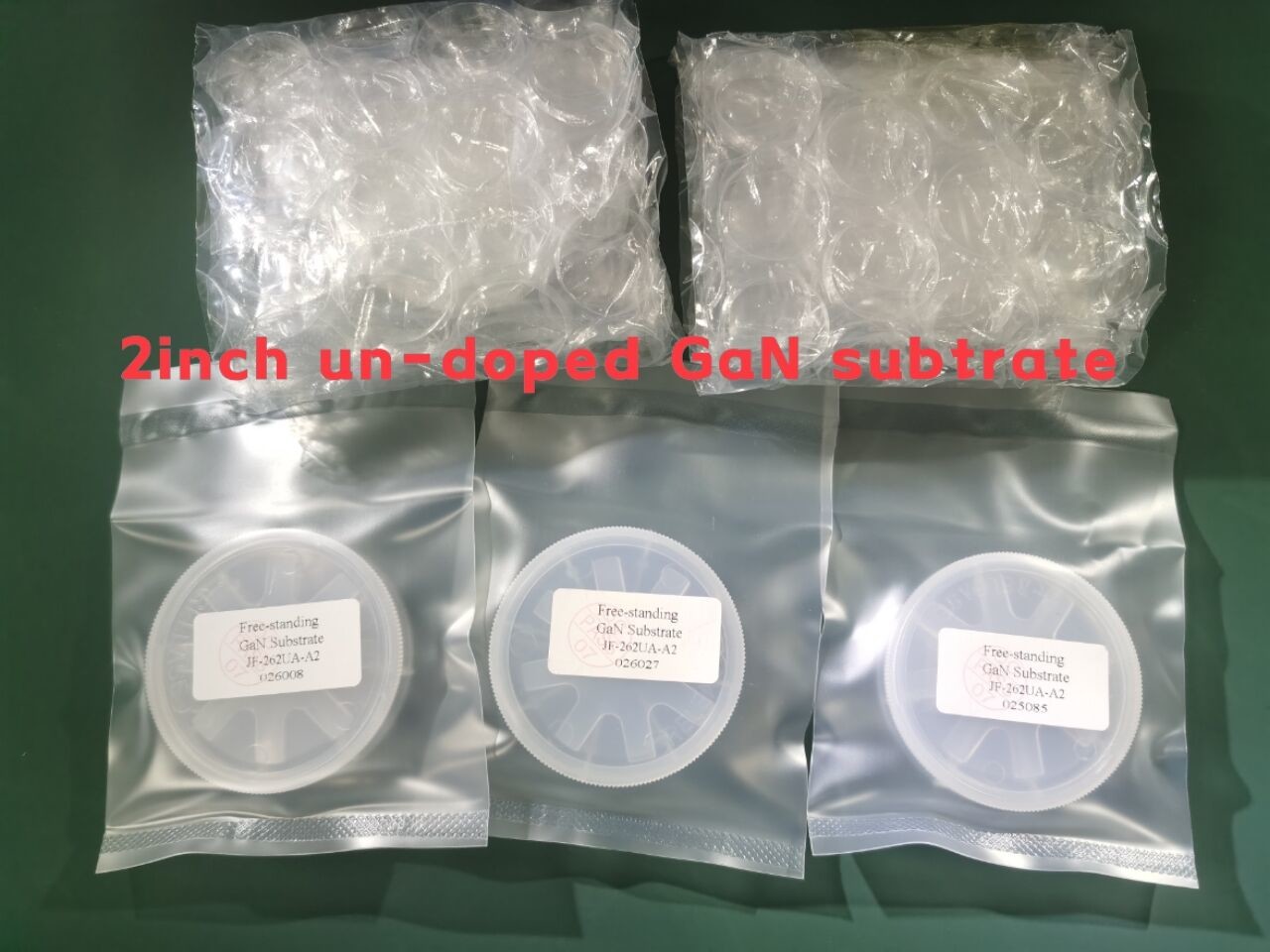
| Packaging Details: | single wafer case by vacuum package |
| Material: | GaN single crystal |
| size: | 2INCH 4inch |
| thickness: | 0.4mm |
| type: | N-type/Un-doped si-doped semi-type |
| Application: | semiconductor Device |
| application: | Powder device |
| surface: | SSP |
| Package: | single wafer container box |
| Company Info. |
| SHANGHAI FAMOUS TRADE CO.,LTD |
| Verified Supplier |
| View Contact Details |
| Product List |
2inch GaN substrates template,GaN wafer for LeD,semiconducting Gallium Nitride Wafer for ld,GaN template, mocvd GaN Wafer,Free-standing GaN Substrates by Customized size,small size GaN wafer for LED, mocvd Gallium Nitride wafer 10x10mm,5x5mm, 10x5mm GaN wafer,Non-Polar Freestanding GaN Substrates(a-plane and m-plane)
4inch 2inch free-standing GaN substrates HVPE GaN Wafers
GaN Wafer Characteristic
Gallium Nitride is one kind of wide-gap compound semiconductors. Gallium Nitride (GaN) substrate is
a high-quality single-crystal substrate. It is made with original HVPE method and wafer processing technology, which has been originally developed for 10+years in China. The features are high crystalline, good uniformity, and superior surface quality. GaN substrates are used for many kinds of applications, for white LED and LD(violet, blue and green) Furthermore, development has progressed for power and high frequency electronic device applications.
Forbidden band width (light emitting and absorption) cover the ultraviolet, visible light and infrared.
Application
GaN can be used in many areas such as LED display, High-energy
Detection and Imaging,
Laser Projection Display, Power Device, etc.
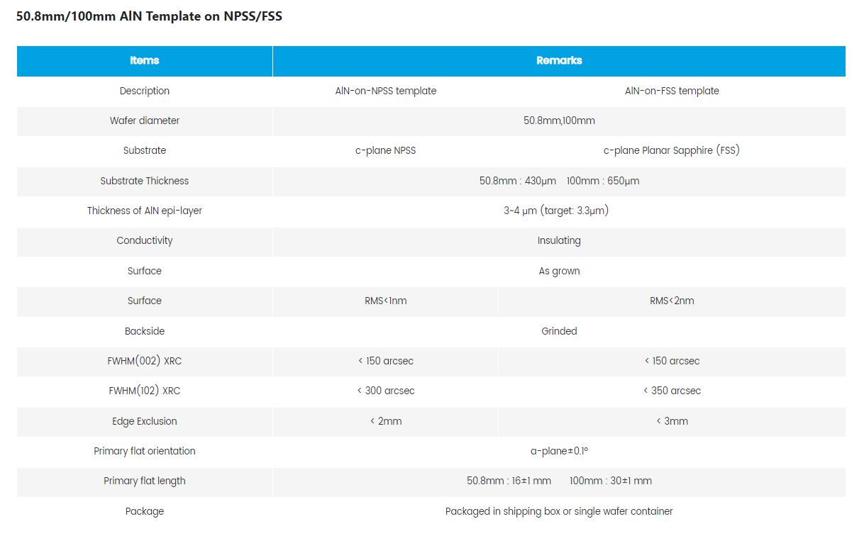
Specification for free-standing GaN wafers
| Size | 2" | 4" | ||
| Diameter | 50.8 mm 士 0.3 mm | 100.0 mm 士 0.3 mm | ||
| Thickness | 400 um 士 30 um | 450 um 士 30 um | ||
| Orientation | (0001) Ga-face c-plane (standard); (000-1) N-face (optional) | |||
| 002 XRD Rocking Curve FWHM | < 100 arcsec | |||
| 102 XRD Rocking Curve FWHM | < 100 arcsec | |||
| Lattice Radius of Curvature | > 10 m (measured at 80% x diameter) | |||
| Offcut Toward m-plane | 0.5° ± 0.15° toward [10-10] @ wafer center | |||
| Offcut Toward Orthogonal a-plane | 0.0° ± 0.15° toward [1-210] @ wafer center | |||
| Offcut In-Plane Direction | The c-plane vector projection points toward the major OF | |||
| Major Orientation Flat Plane | (10-10) m-plane 2° (standard); ±0.1° (optional) | |||
| Major Orientation Flat Length | 16.0 mm ±1 mm | 32.0 mm ± 1 mm | ||
| Minor Orientation Flat Orientation | Ga-face = major OF on bottom and minor OF on left | |||
| Minor Orientation Flat Length | 8.0 mm ± 1 mm | 18.0 mm ± 1 mm | ||
| Edge Bevel | beveled | |||
| TTV (5 mm edge exclusion) | < 15 um | < 30 um | ||
| Warp (5 mm edge exclusion) | < 20 um | < 80 um | ||
| Bow (5 mm edge exclusion) | -10 um to +5 um | -40 um to +20 um | ||
| Front Side Roughness (Sa) | < 0.3 nm (AFM: 10 um x 10 um area) | |||
| < 1.5 nm (WLI: 239 um x 318 um area) | ||||
| Back Side Surface Finish | polished (standard); etch (optional) | |||
| Back Side Roughness (Sa) | polished: < 3 nm (WLI: 239 um x 318 um area) | |||
| etched: 1 um ± 0.5 um (WLI: 239 um x 318 um area) | ||||
| Laser Mark | back side on major flat | |||
| Electrical Properties | Doping | Resistivity | ||
| N-type ⑸ licon) | < 0.02 ohm-cm | |||
| UID | < 0.2 ohm-cm | |||
| Semi-Insulating (Carbon) | > 1E8 ohm-cm | |||
| Pits Grading System | Density (pits/cm2) | 2" (pits) | 4" (pits) | |
| Production | < 0.5 | < 10 | < 40 | |
| Research | < 1.5 | < 30 | < 120 | |
| Dummy | < 2.5 | < 50 | < 200 | |
ABOUT OUR OEM Factory
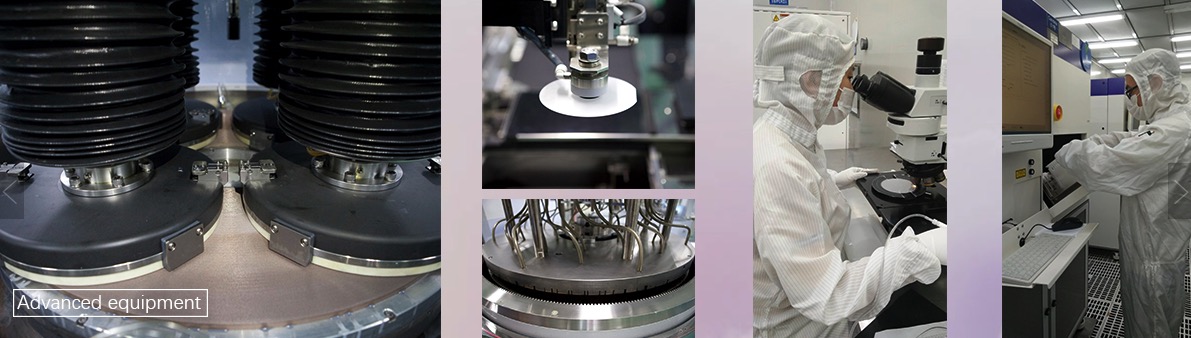
Our Factroy Enterprise Vision
we will provide high quality GaN substrate and application
technology for the industry with our factory.
High quality GaNmaterial is the restraining factor for the
III-nitrides application, e.g. long life
and high stability LDs, high power and high reliability micro-wave
devices, High brightness
and high efficiency, energy-saving LED.
-FAQ –
Q: What you can supply logistics and cost?
(1) We accept DHL, Fedex, TNT, UPS, EMS, SF and etc.
(2) If you have your own express number, it's great.
If not, we could assist you to deliver. Freight=USD25.0(the first
weight) + USD12.0/kg
Q: What's the delivery time?
(1) For the standard products such as 2inch 0.33mm wafer.
For inventory: the delivery is 5 workdays after order.
For customized products: the delivery is 2 or 4 workweeks after
order.
Q: How to pay?
100%T/T, Paypal, West Union, MoneyGram, Secure payment and Trade
Assurance.
Q: What's the MOQ?
(1) For inventory, the MOQ is 5pcs.
(2) For customized products, the MOQ is 5pcs-10pcs.
It depends on quantity and technics.
Q: Do you have inspection report for material?
We can supply ROHS report and reach reports for our products.

|
