| Sign In | Join Free | My ecer.jp |
|
| Sign In | Join Free | My ecer.jp |
|
| Categories | Scientific Lab Equipment |
|---|---|
| Brand Name: | ZMSH |
| Place of Origin: | China |
| MOQ: | 2 |
| Payment Terms: | T/T |
| Countertop Volume:: | 300*300*150 |
| Positioning Accuracy μm:: | +/-5 |
| Repeated Positioning Accuracy μm:: | +/-2 |
| Numerical Control Type:: | DPSS Nd:YAG |
| Company Info. |
| SHANGHAI FAMOUS TRADE CO.,LTD |
| Verified Supplier |
| View Contact Details |
| Product List |
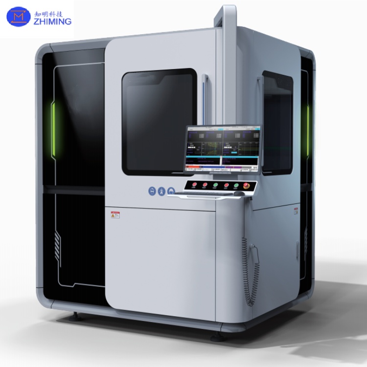
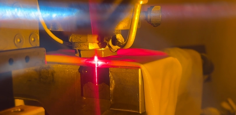
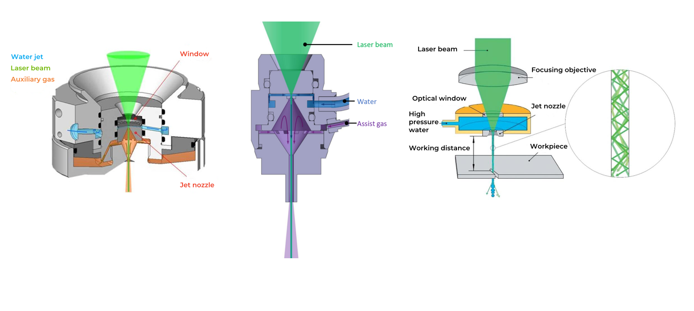
The microjet laser device is a revolutionary precision machining system that achieves thermal damage-free, high-precision material processing by coupling high-energy laser beams to micron-scale liquid jets. The technology is particularly suitable for semiconductor manufacturing, enabling critical processes such as SiC/GaN wafer cutting, TSV drilling, and advanced packaging with sub-micron accuracy (0.5-5μm), while eliminating edging and heat-affected zones (HAZ<1μm) caused by traditional processing. Its unique liquid guiding mechanism not only ensures machining cleanliness (in line with Class 100 standards), but also improves yields by more than 15%, and is now the core equipment for third-generation semiconductor and 3D chip manufacturing.
· High precision and efficiency: Microjet laser technology achieves precise cutting and processing by coupling the laser beam into a high-speed water jet after focusing, avoiding the problems of thermal damage and material deformation in traditional laser processing, while maintaining the cooling of the processing area to ensure high precision and surface finish.
· No material damage and heat affected zones: This technology
utilizes water jet cooling capabilities to create virtually no heat
affected zones or microstructure changes, while removing ablative
debris and keeping surfaces clean.
· Suitable for a variety of materials: metal, ceramics, composite
materials, diamonds, silicon carbide and other hard and brittle
materials, especially in the cutting thickness of up to millimeters
of excellent performance.
· Flexibility and safety: The machine supports multiple modes of
operation (such as 3-axis or 5-axis) and is equipped with a visual
recognition system and autofocus function to improve processing
efficiency and safety
·Environmental protection and energy saving: Compared with traditional laser processing methods, microjet laser technology reduces material loss and energy consumption, in line with the concept of green manufacturing.
| Countertop volume | 300*300*150 | 400*400*200 |
| Linear axis XY | Linear motor. Linear motor | Linear motor. Linear motor |
| Linear axis Z | 150 | 200 |
| Positioning accuracy μm | +/-5 | +/-5 |
| Repeated positioning accuracy μm | +/-2 | +/-2 |
| Acceleration G | 1 | 0.29 |
| Numerical control | 3 axis /3+1 axis /3+2 axis | 3 axis /3+1 axis /3+2 axis |
| Numerical control type | DPSS Nd:YAG | DPSS Nd:YAG |
| Wavelength nm | 532/1064 | 532/1064 |
| Rated power W | 50/100/200 | 50/100/200 |
| Water jet | 40-100 | 40-100 |
| Nozzle pressure bar | 50-100 | 50-600 |
| Dimensions (machine tool) (width * length * height) mm | 1445*1944*2260 | 1700*1500*2120 |
| Size (control cabinet) (W * L * H) | 700*2500*1600 | 700*2500*1600 |
| Weight (equipment) T | 2.5 | 3 |
| Weight (control cabinet) KG | 800 | 800 |
| Processing capability | Surface roughness Ra≤1.6um Opening speed ≥1.25mm/s Circumference cutting ≥6mm/s Linear cutting speed ≥50mm/s | Surface roughness Ra≤1.2um Opening speed ≥1.25mm/s Circumference cutting ≥6mm/s Linear cutting speed ≥50mm/s |
For gallium nitride crystal, ultra-wide band gap semiconductor materials (diamond/Gallium oxide), aerospace special materials, LTCC carbon ceramic substrate, photovoltaic, scintillator crystal and other materials processing. Note: Processing capacity varies depending on material characteristics | ||
1.Aerospace and semiconductor: used for silicon carbide ingot
cutting, gallium nitride single crystal cutting, etc., to solve the
processing problems of aerospace special materials.
2. Medical devices: Used for precision machining of high-quality
medical device parts, such as implants, catheters, scalpels, etc.,
with high biocompatibility and low post-processing requirements.
3. Consumer electronics and AR equipment: achieve high-precision
cutting and thinness in AR lens processing, and promote the
large-scale application of new materials such as silicon carbide
lenses.
4. Industrial manufacturing: widely used in metal, ceramics,
composite materials complex parts processing, such as clock parts,
electronic components, etc.
1. Q: What is microjet laser technology?
A: Microjet laser technology combines laser precision with liquid
cooling to enable ultra-clean, high-accuracy material processing.
2. Q: What are the benefits of microjet laser in semiconductor
manufacturing?
A: It eliminates thermal damage and chipping while cutting/drilling
fragile materials like SiC and GaN wafers.

|
