| Sign In | Join Free | My ecer.jp |
|
| Sign In | Join Free | My ecer.jp |
|
| Categories | SiC Wafer |
|---|---|
| Brand Name: | PAM-XIAMEN |
| MOQ: | 1-10,000pcs |
| Price: | By Case |
| Payment Terms: | T/T |
| Supply Ability: | 10,000 wafers/month |
| Delivery Time: | 5-50 working days |
| Place of Origin: | China |
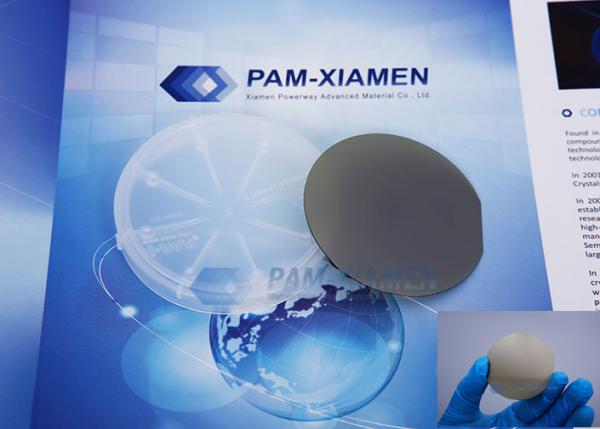
PAM-XIAMEN offers semiconductor silicon carbide wafers,6H SiC and 4H SiC in different quality grades for researcher and industry manufacturers. We has developed SiC crystal growth technology and SiC crystal wafer processing technology,established a production line to manufacturer SiC substrate,Which is applied in GaN epitaxy device,power devices,high-temperature device and optoelectronic Devices. As a professional company invested by the leading manufacturers from the fields of advanced and high-tech material research and state institutes and China’s Semiconductor Lab,we are devoted to continuously improve the quality of currently substrates and develop large size substrates.
Here shows detail specification:
SILICON CARBIDE MATERIAL PROPERTIES
| Polytype | Single Crystal 4H | Single Crystal 6H |
| Lattice Parameters | a=3.076 Å | a=3.073 Å |
| c=10.053 Å | c=15.117 Å | |
| Stacking Sequence | ABCB | ABCACB |
| Band-gap | 3.26 eV | 3.03 eV |
| Density | 3.21 · 103 kg/m3 | 3.21 · 103 kg/m3 |
| Therm. Expansion Coefficient | 4-5×10⁻⁶/K | 4-5×10⁻⁶/K |
| Refraction Index | no = 2.719 | no = 2.707 |
| ne = 2.777 | ne = 2.755 | |
| Dielectric Constant | 9.6 | 9.66 |
| Thermal Conductivity | 490 W/mK | 490 W/mK |
| Break-Down Electrical Field | 2-4 · 108 V/m | 2-4 · 108 V/m |
| Saturation Drift Velocity | 2.0 · 105 m/s | 2.0 · 105 m/s |
| Electron Mobility | 800 cm2/V·S | 400 cm2/V·S |
| hole Mobility | 115 cm2/V·S | 90 cm2/V·S |
| Mohs Hardness | ~9 | ~9 |
6H N-TYPE SiC, 2″(50.8mm)WAFER SPECIFICATION
| SUBSTRATE PROPERTY | S6H-51-N-PWAM-250 S6H-51-N-PWAM-330 S6H-51-N-PWAM-430 |
| Description | A/B Production Grade C/D Research Grade D Dummy Grade 6H SiC Substrate |
| Polytype | 6H |
| Diameter | (50.8 ± 0.38) mm |
| Thickness | (250 ± 25) μm (330 ± 25) μm (430 ± 25) μm |
| Carrier Type | n-type |
| Dopant | Nitrogen |
| Resistivity (RT) | 0.02 ~ 0.1 Ω·cm |
| Surface Roughness | < 0.5 nm (Si-face CMP Epi-ready); <1 nm (C- face Optical polish) |
| FWHM | A<30 arcsec B/C/D <50 arcsec |
| Micropipe Density | A+≤1cm-2 A≤10cm-2 B≤30cm-2 C≤50cm-2 D≤100cm-2 |
| Surface Orientation | |
| On axis | <0001>± 0.5° |
| Off axis | 3.5° toward <11-20>± 0.5° |
| Primary flat orientation | Parallel {1-100} ± 5° |
| Primary flat length | 16.00 ± 1.70 mm |
| Secondary flat orientation | Si-face:90° cw. from orientation flat ± 5° |
| C-face:90° ccw. from orientation flat ± 5° | |
| Secondary flat length | 8.00 ± 1.70 mm |
| Surface Finish | Single or double face polished |
| Packaging | Single wafer box or multi wafer box |
| Usable area | ≥ 90 % |
| Edge exclusion | 1 mm |
4H SEMI-INSULATING SiC, 2″(50.8mm)WAFER SPECIFICATION
(High-Purity Semi-Insulating(HPSI) SiC substrate is available)
| SUBSTRATE PROPERTY | S4H-51-SI-PWAM-250 S4H-51-SI-PWAM-330 S4H-51-SI-PWAM-430 |
| Description | A/B Production Grade C/D Research Grade D Dummy Grade 4H SEMI Substrate |
| Polytype | 4H |
| Diameter | (50.8 ± 0.38) mm |
| Thickness | (250 ± 25) μm (330 ± 25) μm (430 ± 25) μm |
| Resistivity (RT) | >1E5 Ω·cm |
| Surface Roughness | < 0.5 nm (Si-face CMP Epi-ready); <1 nm (C- face Optical polish) |
| FWHM | A<30 arcsec B/C/D <50 arcsec |
| Micropipe Density | A+≤1cm-2 A≤10cm-2 B≤30cm-2 C≤50cm-2 D≤100cm-2 |
| Surface Orientation | |
| On axis <0001>± 0.5° | |
| Off axis 3.5° toward <11-20>± 0.5° | |
| Primary flat orientation | Parallel {1-100} ± 5° |
| Primary flat length | 16.00 ± 1.70 mm |
| Secondary flat orientation Si-face:90° cw. from orientation flat ± 5° | |
| C-face:90° ccw. from orientation flat ± 5° | |
| Secondary flat length | 8.00 ± 1.70 mm |
| Surface Finish | Single or double face polished |
| Packaging | Single wafer box or multi wafer box |
| Usable area | ≥ 90 % |
| Edge exclusion | 1 mm |
4H N-type or Semi-insulating SIC,5mm*5mm, 10mm*10mm WAFER SPECIFICATION : Thickness:330μm/430μm
4H N-type or Semi-insulating SIC,15mm*15mm, 20mm*20mm WAFER SPECIFICATION: Thickness:330μm/430μm
4H N-TYPE SiC, 2″(50.8mm)WAFER SPECIFICATION
| SUBSTRATE PROPERTY | S4H-51-N-PWAM-330 S4H-51-N-PWAM-430 | |
| Description | A/B Production Grade C/D Research Grade D Dummy Grade 4H SiC Substrate | |
| Polytype | 4H | |
| Diameter | (50.8 ± 0.38) mm | |
| Thickness | (250 ± 25) μm (330 ± 25) μm (430 ± 25) μm | |
| Carrier Type | n-type | |
| Dopant | Nitrogen | |
| Resistivity (RT) | 0.012 – 0.0028 Ω·cm | |
| Surface Roughness | < 0.5 nm (Si-face CMP Epi-ready); <1 nm (C- face Optical polish) | |
| FWHM | A<30 arcsec B/C/D <50 arcsec | |
| Micropipe Density | A+≤1cm-2 A≤10cm-2 B≤30cm-2 C≤50cm-2 D≤100cm-2 | |
| Surface Orientation | ||
| On axis | <0001>± 0.5° | |
| Off axis | 4°or 8° toward <11-20>± 0.5° | |
| Primary flat orientation | Parallel {1-100} ± 5° | |
| Primary flat length | 16.00 ± 1.70) mm | |
| Secondary flat orientation | Si-face:90° cw. from orientation flat ± 5° | |
| C-face:90° ccw. from orientation flat ± 5° | ||
| Secondary flat length | 8.00 ± 1.70 mm | |
| Surface Finish | Single or double face polished | |
| Packaging | Single wafer box or multi wafer box | |
| Usable area | ≥ 90 % | |
| Edge exclusion | 1 mm | |
4H N-TYPE SiC, 3″(76.2mm)WAFER SPECIFICATION
| SUBSTRATE PROPERTY | S4H-76-N-PWAM-330 S4H-76-N-PWAM-430 |
| Description | A/B Production Grade C/D Research Grade D Dummy Grade 4H SiC Substrate |
| Polytype | 4H |
| Diameter | (76.2 ± 0.38) mm |
| Thickness | (350 ± 25) μm (430 ± 25) μm |
| Carrier Type | n-type |
| Dopant | Nitrogen |
| Resistivity (RT) | 0.015 – 0.028Ω·cm |
| Surface Roughness | < 0.5 nm (Si-face CMP Epi-ready); <1 nm (C- face Optical polish) |
| FWHM | A<30 arcsec B/C/D <50 arcsec |
| Micropipe Density | A+≤1cm-2 A≤10cm-2 B≤30cm-2 C≤50cm-2 D≤100cm-2 |
| TTV/Bow /Warp | <25μm |
| Surface Orientation | |
| On axis | <0001>± 0.5° |
| Off axis | 4°or 8° toward <11-20>± 0.5° |
| Primary flat orientation | <11-20>±5.0° |
| Primary flat length | 22.22 mm±3.17mm |
| 0.875″±0.125″ | |
| Secondary flat orientation | Si-face:90° cw. from orientation flat ± 5° |
| C-face:90° ccw. from orientation flat ± 5° | |
| Secondary flat length | 11.00 ± 1.70 mm |
| Surface Finish | Single or double face polished |
| Packaging | Single wafer box or multi wafer box |
| Scratch | None |
| Usable area | ≥ 90 % |
| Edge exclusion | 2mm |
4H SEMI-INSULATING SiC, 3″(76.2mm)WAFER SPECIFICATION
(High Purity Semi-Insulating(HPSI) SiC substrate is available)
| SUBSTRATE PROPERTY | S4H-76-N-PWAM-330 S4H-76-N-PWAM-430 |
| Description | A/B Production Grade C/D Research Grade D Dummy Grade 4H SiC Substrate |
| Polytype | 4H |
| Diameter | (76.2 ± 0.38) mm |
| Thickness | (350 ± 25) μm (430 ± 25) μm |
| Carrier Type | semi-insulating |
| Dopant | V |
| Resistivity (RT) | >1E5 Ω·cm |
| Surface Roughness | < 0.5 nm (Si-face CMP Epi-ready); <1 nm (C- face Optical polish) |
| FWHM | A<30 arcsec B/C/D <50 arcsec |
| Micropipe Density | A+≤1cm-2 A≤10cm-2 B≤30cm-2 C≤50cm-2 D≤100cm-2 |
| TTV/Bow /Warp | <25μm |
| Surface Orientation | |
| On axis | <0001>± 0.5° |
| Off axis | 4°or 8° toward <11-20>± 0.5° |
| Primary flat orientation | <11-20>±5.0° |
| Primary flat length | 22.22 mm±3.17mm |
| 0.875″±0.125″ | |
| Secondary flat orientation | Si-face:90° cw. from orientation flat ± 5° |
| C-face:90° ccw. from orientation flat ± 5° | |
| Secondary flat length | 11.00 ± 1.70 mm |
| Surface Finish | Single or double face polished |
| Packaging | Single wafer box or multi wafer box |
| Scratch | None |
| Usable area | ≥ 90 % |
| Edge exclusion | 2mm |
4H N-TYPE SiC, 4″(100mm)WAFER SPECIFICATION
| SUBSTRATE PROPERTY | S4H-100-N-PWAM-330 S4H-100-N-PWAM-430 |
| Description | A/B Production Grade C/D Research Grade D Dummy Grade 4H SiC Substrate |
| Polytype | 4H |
| Diameter | (100.8 ± 0.38) mm |
| Thickness | (350 ± 25) μm (430 ± 25) μm |
| Carrier Type | n-type |
| Dopant | Nitrogen |
| Resistivity (RT) | 0.015 – 0.028Ω·cm |
| Surface Roughness | < 0.5 nm (Si-face CMP Epi-ready); <1 nm (C- face Optical polish) |
| FWHM | A<30 arcsec B/C/D <50 arcsec |
| Micropipe Density | A+≤1cm-2 A≤10cm-2 B≤30cm-2 C≤50cm-2 D≤100cm-2 |
| TTV/Bow /Warp | <45μm |
| Surface Orientation | |
| On axis | <0001>± 0.5° |
| Off axis | 4°or 8° toward <11-20>± 0.5° |
| Primary flat orientation | <11-20>±5.0° |
| Primary flat length | 32.50 mm±2.00mm |
| Secondary flat orientation | Si-face:90° cw. from orientation flat ± 5° |
| C-face:90° ccw. from orientation flat ± 5° | |
| Secondary flat length | 18.00 ± 2.00 mm |
| Surface Finish | Single or double face polished |
| Packaging | Single wafer box or multi wafer box |
| Scratch | None |
| Usable area | ≥ 90 % |
| Edge exclusion | 2mm |
4H N-type or semi-insulating SIC,5mm*5mm, 10mm*10mm WAFER SPECIFICATION: Thickness:330μm/430μm
4H N-type or semi-insulating SIC,15mm*15mm, 20mm*20mm WAFER SPECIFICATION:Thickness:330μm/430μm
a-plane SiC Wafer, size: 40mm*10mm,30mm*10mm,20mm*10mm,10mm*10mm,specs below:
6H/4H N type Thickness:330μm/430μm or custom
6H/4H Semi-insulating Thickness:330μm/430μm or custom
4H SiC,SEMI-INSULATING, 4″(100mm)WAFER SPECIFICATION
(High-Purity Semi-Insulating(HPSI) SiC substrate is available)
| SUBSTRATE PROPERTY | S4H-100-SI-PWAM-350 S4H-100-SI-PWAM-500 | |
| Description | A/B Production Grade C/D Research Grade D Dummy Grade 4H SiC Substrate | |
| Polytype | 4H | |
| Diameter | (100 ± 0.5) mm | |
| Thickness | (350 ± 25) μm (500 ± 25) μm | |
| Carrier Type | Semi-insulating | |
| Dopant | V | |
| Resistivity (RT) | >1E5 Ω·cm | |
| Surface Roughness | < 0.5 nm (Si-face CMP Epi-ready); <1 nm (C- face Optical polish) | |
| FWHM | A<30 arcsec B/C/D <50 arcsec | |
| Micropipe Density | A≤5cm-2 B≤15cm-2 C≤50cm-2 D≤100cm-2 | |
| TTV/Bow /Warp | TTV<10μm;TTV< 25μm;WARP<45μm | |
| Surface Orientation | ||
| On axis | <0001>± 0.5° | |
| Off axis | None | |
| Primary flat orientation | <11-20>±5.0° | |
| Primary flat length | 32.50 mm±2.00mm | |
| Secondary flat orientation | Si-face:90° cw. from orientation flat ± 5° | |
| C-face:90° ccw. from orientation flat ± 5° | ||
| Secondary flat length | 18.00 ± 2.00 mm | |
| Surface Finish | Double face polished | |
| Packaging | Single wafer box or multi wafer box | |
| Scratches | <8 scratches to 1 x wafer diameter with total cumulative length | |
| Cracks | None | |
| Usable area | ≥ 90 % | |
| Edge exclusion | 2mm | |
4H SiC,N-TYPE , 6″(150mm)WAFER SPECIFICATION
| SUBSTRATE PROPERTY | S4H-150-N-PWAM-350 | |
| Description | Dummy Grade 2 | |
| Polytype | 4H | |
| Diameter | (150 ± 0.2) mm | |
| Thickness | (350 ± 25) μm | |
| Carrier Type | n-type | |
| Dopant | Nitrogen | |
| Resistivity (RT) | 0.015 – 0.028Ω·cm | |
| Surface Roughness | < 0.5 nm (Si-face CMP Epi-ready); <1 nm (C- face Optical polish) | |
| Micropipe Density | N/A | |
| TTV | ≤30μm | |
| Bow | ≤120μm | |
| Warp | ≤150μm | |
| Surface Orientation | ||
| Off axis | 4° toward <11-20>± 0.5° | |
| Primary flat orientation | <10-10>±5.0° | |
| Primary flat length | 47.50 mm±2.50mm | |
| Surface Finish | Double face polished | |
| Edge exclusion | 3mm | |
| Packaging | Single wafer box or multi wafer box | |
Please see below sub-catalogue:
|
