| Sign In | Join Free | My ecer.jp |
|
| Sign In | Join Free | My ecer.jp |
|
| Categories | SiC Wafer |
|---|---|
| Brand Name: | PAM-XIAMEN |
| Place of Origin: | China |
| MOQ: | 1-10,000pcs |
| Price: | By Case |
| Payment Terms: | T/T |
| Supply Ability: | 10,000 wafers/month |
| Delivery Time: | 5-50 working days |
| name: | 6H N Type SIC Wafer |
| Grade: | Production Grade |
| Description: | Production Grade 6H SiC Substrate |
| Carrier Type: | n-type |
| Diameter: | (50.8 ± 0.38) mm |
| Thickness: | (250 ± 25) μm (330 ± 25) μm (430 ± 25) μm |
On-Axis 6H N Type SiC(Silicon Carbide) Wafer, Production Grade,Epi Ready,2”Size
PAM-XIAMEN provides high quality single crystal SiC (Silicon Carbide)waferfor electronic and optoelectronic industry. SiC wafer is a next generation semiconductor materialwith unique electrical properties and excellent thermal properties for high temperature and high power device application. SiC wafer can be supplied in diameter 2~6 inch, both 4H and 6H SiC , N-type , Nitrogen doped , and semi-insulating type available. Please contact us for more information.
SILICON CARBIDE MATERIAL PROPERTIES
| Polytype | Single Crystal 4H | Single Crystal 6H |
| Lattice Parameters | a=3.076 Å | a=3.073 Å |
| c=10.053 Å | c=15.117 Å | |
| Stacking Sequence | ABCB | ABCACB |
| Band-gap | 3.26 eV | 3.03 eV |
| Density | 3.21 · 103 kg/m3 | 3.21 · 103 kg/m3 |
| Therm. Expansion Coefficient | 4-5×10⁻⁶/K | 4-5×10⁻⁶/K |
| Refraction Index | no = 2.719 | no = 2.707 |
| ne = 2.777 | ne = 2.755 | |
| Dielectric Constant | 9.6 | 9.66 |
| Thermal Conductivity | 490 W/mK | 490 W/mK |
| Break-Down Electrical Field | 2-4 · 108 V/m | 2-4 · 108 V/m |
| Saturation Drift Velocity | 2.0 · 105 m/s | 2.0 · 105 m/s |
| Electron Mobility | 800 cm2/V·S | 400 cm2/V·S |
| hole Mobility | 115 cm2/V·S | 90 cm2/V·S |
| Mohs Hardness | ~9 | ~9 |
6H N Type SiC Wafer, Production Grade,Epi Ready,2”Size
| SUBSTRATE PROPERTY | S6H-51-N-PWAM-250 S6H-51-N-PWAM-330 S6H-51-N-PWAM-430 |
| Description | Production Grade 6H SiC Substrate |
| Polytype | 6H |
| Diameter | (50.8 ± 0.38) mm |
| Thickness | (250 ± 25) μm (330 ± 25) μm (430 ± 25) μm |
| Carrier Type | n-type |
| Dopant | Nitrogen |
| Resistivity (RT) | 0.02 ~ 0.1 Ω·cm |
| Surface Roughness | < 0.5 nm (Si-face CMP Epi-ready); <1 nm (C- face Optical polish) |
| FWHM | <30 arcsec <50 arcsec |
| Micropipe Density | A+≤1cm-2 A≤10cm-2 B≤30cm-2 C≤50cm-2 D≤100cm-2 |
| Surface Orientation | |
| On axis | <0001>± 0.5° |
| Off axis | 3.5° toward <11-20>± 0.5° |
| Primary flat orientation | Parallel {1-100} ± 5° |
| Primary flat length | 16.00 ± 1.70 mm |
| Secondary flat orientation | Si-face:90° cw. from orientation flat ± 5° |
| C-face:90° ccw. from orientation flat ± 5° | |
| Secondary flat length | 8.00 ± 1.70 mm |
| Surface Finish | Single or double face polished |
| Packaging | Single wafer box or multi wafer box |
| Usable area | ≥ 90 % |
| Edge exclusion | 1 mm |
SiC Crystal Structure
SiC Crystal has many different crystal structures,which is called polytypes.The most common polytypes of SiC presently being developed for electronics are the cubic 3C-SiC, the hexagonal 4H-SiC and 6H-SiC, and the rhombohedral 15R-SiC. These polytypes are characterized by the stacking sequence of the biatom layers of the SiC structure.For more details, please enquire our engineer team.
Stacking Sequence:
If we are going to make a laminated structure, we must know the thickness of each ply and the angle of each ply traditionally in degrees defined from the top layer down.
Rough measure of the resistance of a smooth surface to scratching or abrasion, expressed in terms of a scale devised(1812)by the German mineralogist Friedrich Mohs. The Mohs hardness of a mineral is determined by observing whether its surface is scratched by a substance of known or defined hardness.
Density:
The mass density or density of a material is its mass per unit volume. The symbol
most often used for density is ρ (the lower case Greek letter rho).
Mathematically, density is defined as mass divided by volume: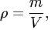

|
