| Sign In | Join Free | My ecer.jp |
|
| Sign In | Join Free | My ecer.jp |
|
| Categories | Burn In Test PCB |
|---|---|
| Brand Name: | TOPCBS |
| Model Number: | BIB and test Boards |
| Certification: | UL94V0 |
| Place of Origin: | Suzhou China |
| MOQ: | Negotiation |
| Price: | Negotiation |
| Payment Terms: | T/T |
| Supply Ability: | 10000unit per month |
| Delivery Time: | 10-14working days |
| Packaging Details: | 20units per package box size 20*15*10cm |
| Layer count: | 12Layer |
| Raw material: | High Tg FR4 |
| Finished Treatment: | Immerion Gold + OSP |
| Pitch Size: | 0.3mm |
| Board thickness: | 0.7mm |
| Line width/space: | 75um/100um |
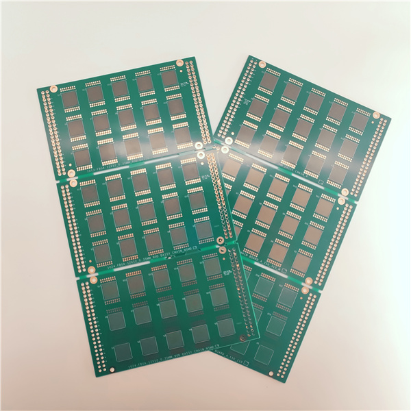
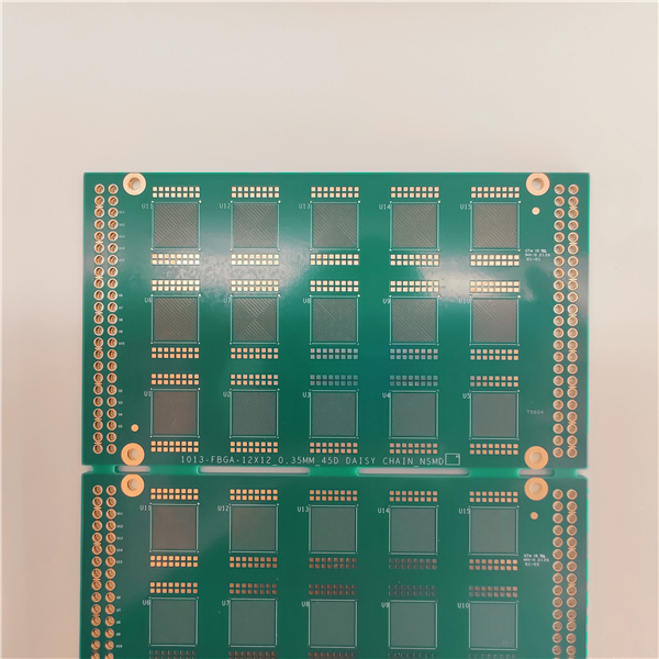
0.3 pitch 12Layer HDI PCBs for Burn in boards and semiconductor Test boards / thin board
A functional test is used as a final manufacturing step to validate that a PCB is free of defects. If untested, it may adversely affect the correct functioning of a device after integrating these boards into complete systems. In simple terms, a functional test verifies a PCB functionality and its behavior. PCB functional testing consists of a number of tests for qualifying board functionality, covering everything from checking for signal behavior to short circuits.
Apart from other tests that can be performed on any PCB, functional testing provides the most comprehensive view of a signal behavior. This goes beyond in-circuit testing, wherein individual components are examined after being soldered on a PCB. In contrast, PCB functional testing provides pass/fail determination on finished PCBs before shipping.
1 . Descriptions:
What is a BIB ?
A burn-in board is a printed circuit board that is used in the burn-in process. The components added to the board are stressed using extreme heat to highlight any failures. Once the stress tests have been completed engineers will analyse the results to make sure everything is working within the correct parameters.
2 . Specifications:
| Name | 0.3 pitch 12Layer HDI PCBs for Burn in boards and semiconductor Test boards |
| Number of Layers | 12 |
| Quality Grade | IPC 6012 Class 2,IPC 6012 Class 3 |
| Material | IT180 |
| Thickness | 0.7mm |
| Min Track/Spacing | 75um/75um |
| Min Hole Size | Laser 75um |
| Solder Mask | Green |
| Silkscreen | White |
| Surface Finish | Immersion gold + OSP |
| Finished Copper | 12um |
| Production time | 10-21 working days |
| Lead time | 2-3 days |

|
