| Sign In | Join Free | My ecer.jp |
|
| Sign In | Join Free | My ecer.jp |
|
| Categories | Burn In Test PCB |
|---|---|
| Brand Name: | TOPCBS |
| Model Number: | BIB and test Boards |
| Certification: | UL94V0 |
| Place of Origin: | Suzhou China |
| MOQ: | Negotiation |
| Price: | Negotiation |
| Payment Terms: | T/T |
| Supply Ability: | 10000unit per month |
| Delivery Time: | 10-14working days |
| Packaging Details: | 20units per package box size 20*15*10cm |
| Layer count: | 12Layer |
| Raw material: | High Tg FR4 |
| Finished Treatment: | Immerion Gold + OSP |
| Pitch Size: | 0.3mm |
| Board thickness: | 0.7mm |
| Line width/space: | 75um/100um |
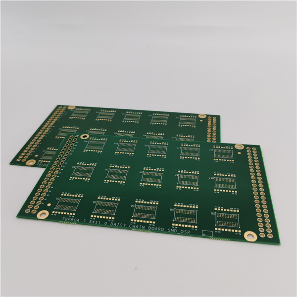
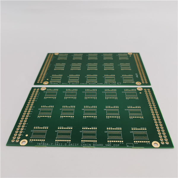
12Layer HDI PCBs for Burn in boards and semiconductor Test boards / thin board
Burn-in is an accepted practice for detecting early failures in a population of semiconductor devices. It usually requires the electrical testing of a product, using an expected operating electrical cycle (extreme of operating condition), typically over a time period of 48-168 hours. Alternatively, thermal (e.g. 125°C for 168 hours) or environmental stress screening (e.g. 20 cycles from -10 to 70°C ramped at +°C/mm) is used. Burn-in is applied to products as they are made, to detect early failures caused by faults in manufacturing practice.
1 . Descriptions:
What is a BIB ?
A burn-in board is a printed circuit board that is used in the burn-in process. The components added to the board are stressed using extreme heat to highlight any failures. Once the stress tests have been completed engineers will analyse the results to make sure everything is working within the correct parameters.
2 . Specifications:
| Name | 12Layer HDI PCBs for Burn in boards and semiconductor Test boards |
| Number of Layers | 12 |
| Quality Grade | IPC 6012 Class 2,IPC 6012 Class 3 |
| Material | IT180 |
| Thickness | 0.7mm |
| Min Track/Spacing | 75um/75um |
| Min Hole Size | Laser 75um |
| Solder Mask | Green |
| Silkscreen | White |
| Surface Finish | Immersion gold + OSP |
| Finished Copper | 12um |
| Production time | 10-21 working days |
| Lead time | 2-3 days |

|
