| Sign In | Join Free | My ecer.jp |
|
| Sign In | Join Free | My ecer.jp |
|
| Categories | Half Hole PCB |
|---|---|
| Brand Name: | WITGAIN PCB |
| Model Number: | Half hole PCB0001 |
| Certification: | UL |
| Place of Origin: | Guangdong China |
| MOQ: | 1 pcs/lot |
| Price: | negotiable |
| Payment Terms: | T/T |
| Supply Ability: | 100k pcs/month |
| Delivery Time: | 20 days |
| Packaging Details: | Vacuum bubble bag packaging |
| Material: | FR4 TG>150 |
| No of layers: | 4 Layer |
| Solder mask colour: | Blue Solder Mask |
| Surface technics: | ENIG |
| Min Lind Space&Width:: | 4/4mil |
| Company Info. |
| Witgain Technology Limited |
| View Contact Details |
| Product List |
4 Layer Half Plated Hole PCB Bluetooth Module 0.8MM Board Thickness Cusomized
Board Info:
1 Part NO: Half hole PCB0001
2 Layer Count: 4 Layer PCB
3 Finished Board Thickness: 0.8 MM tolerance is +/-0.1MM
4 Copper Thickness: 1/H/H/1 OZ
5 Min Lind Space&Width: 4/4mil
6 Application Area: Bluetooth Module
Our Capabilities:
| NO | Item | Capability |
| 1 | Layer Count | 1-24 Layers |
| 2 | Board Thickness | 0.1mm-6.0mm |
| 3 | Finished Board Max Size | 700mm*800mm |
| 4 | Finished Board Thickness Tolerance | +/-10% +/-0.1(<1.0mm) |
| 5 | Warp | <0.7% |
| 6 | Major CCL Brand | KB/NanYa/ITEQ/ShengYi/Rogers Etc |
| 7 | Material Type | FR4,CEM-1,CEM-3,Aluminum,Copper, Ceramic, PI, PET |
| 8 | Drill Hole Diameter | 0.1mm-6.5mm |
| 9 | Out Layer Copper Thickness | 1/2OZ-8OZ |
| 10 | Inner Layer Copper Thickness | 1/3OZ-6OZ |
| 11 | Aspect Ratio | 10:1 |
| 12 | PTH Hole Tolerance | +/-3mil |
| 13 | NPTH Hole Tolerance | +/-1mil |
| 14 | Copper Thickness of PTH Wall | >10mil(25um) |
| 15 | Line Width And Space | 2/2mil |
| 16 | Min Solder Mask Bridge | 2.5mil |
| 17 | Solder Mask Alignment Tolerance | +/-2mil |
| 18 | Dimension Tolerance | +/-4mil |
| 19 | Max Gold Thickness | 200u'(0.2mil) |
| 20 | Thermal Shock | 288℃, 10s, 3 times |
| 21 | Impedance Control | +/-10% |
| 22 | Test Capability | PAD Size min 0.1mm |
| 23 | Min BGA | 7mil |
| 24 | Surface Treatment | OSP, ENIG,HASL, Plating Gold, Carbon Oil,Peelable Mask etc |
FAQ:
Q1: What is the Comparative Tracking Index (CTI) or Proof Tracking Index (PTI) of the PCB base material?
A1:
Comparative Tracking Index (CTI) is the extent to which the insulating material of the PCB can resist the unwanted current to flow between traces on the board. It is a measure of the ability of the PCB substrate to withstand any breakdown between two tracks on the PCB surface. It is used to assess the proportionate resistance of the PCB base material and helps calculate the high-voltage isolation values between the tracks. The CTI / PTI value indicates how resistant the PCB material is against environmental influences such as dirt and moisture. The higher the value, the more resistant the material is. The default CTI value for FR4 is 175 and goes up to 600 on special materials. The CTI / PTI value is determined using standard test methods.
Tracking resistance is the resistance offered by the PCB trace against the current flow. The higher the number of components placed on the PCB board the higher is its overall packing density, this leads to smaller trace spacings. Therefore, the CTI / PTI value in the PCB base material is of prime importance. These values help to deduce the overall PCB tracking resistance.
These values give an estimation for leakage or short-circuit as trace spacing becomes small due to the increased number of components. As per the IEC standard, the smaller CTI grade substrate offers good resistance to the electrical breakdown. CTI is a critical number while selecting a PCB material. Normal FR-4 ranges from 175 to 225V. IEC has prescribed three of the following classes for PCB CTI calculation:
| Comparative Tracking Index (CTI) in Volts | Class |
| 600 <= CTI | I |
| 400 <= CTI < 600 | II |
| 175 <= CTI < 400 | IIIA |
| 100 <= CTI < 175 | IIIB |
Understanding CTI with respect to PCB routing:
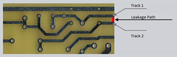
When two PCB traces run in parallel, the dielectric material should not breakdown at any time and both traces should be able to carry current without any problem. The chance of dielectric breaking down and the traces having a direct short is very less. The dielectric ensures that resistance is present between the two traces. One of the primary reasons why the two traces might have leakage current is due to the impurities forming between traces, environmental conditions, voltage applied, and temperature..
CTI is the measurement of the susceptibility of the PCB’s insulating material to the electrical breakdown. Mathematically, CTI is that voltage, which results in failure by breakdown after 50 drops of 0.1 percent ammonium chloride solution have fallen on the material.
Creepage Distance and CTI Value:
Creepage distance is the shortest path available between two PCB conductors measured along the surface of the insulation. Depending upon the CTI value of the PCB base material, the creepage value will differ. If the CTI value is higher, then the minimum creepage value is required. In short, high a CTI value indicates closeness between the PCB conductors.

|
