| Sign In | Join Free | My ecer.jp |
|
| Sign In | Join Free | My ecer.jp |
|
| Categories | Half Hole PCB |
|---|---|
| Brand Name: | WITGAIN PCB |
| Model Number: | Half hole PCB0011 |
| Certification: | UL |
| Place of Origin: | China |
| MOQ: | 1 pcs/lot |
| Price: | negotiable |
| Payment Terms: | T/T |
| Supply Ability: | 100k pcs/month |
| Delivery Time: | 20 days |
| Packaging Details: | Vacuum bubble bag packaging |
| PCB Kind: | 4 Layer PCB |
| Impedance Control: | 50 Ohm |
| Material Kind:: | FR4 TG150 |
| PCB Thickness:: | 1.0 MM |
| Surface technics:: | ENIG |
| PCB Size: | 97.55 mm* 97 mm/25pcs |
| Company Info. |
| Witgain Technology Limited |
| View Contact Details |
| Product List |
Half Hole PCB 4 Layer Immersion Gold 1.0 MM Thickness
Board Info:
1 Part NO: Half hole PCB0010
2 Layer Count: 4 Layer PCB
3 Finished Board Thickness: 1.0 MM tolerance is +/-0.1MM
4 Solder Mask: Green
5 Min Lind Space&Width: 4/4 mil
6 Application Area: Blue-tooth Module
7 Drillings: L1-L4 0.2MM
8 BGA Size: 0.3MM
9 Surface Treatment: immersion gold
10 PCB Size: 97.55 mm* 97 mm/25pcs
11 Impedance control: 50 ohm
Our Product Categories:
1 FR4 substrate PCB : 2 Layer Printed Circuit Board, 4 Layer PCB, 6 Layer PCB, 8 Layer PCB, 10 Layer PCB, 12 Layer PCB, 14 Layer PCB, 16 Layer PCB, 18 Layer PCB, 20 Layer PCB, 22 Layer PCB, 24 Layer PCB, HDI PCB, High frequency PCB.
2 Aluminum Substrate pcb: 1 Layer Aluminum PCB, 2 Layer Aluminum PCB, 4 Layer Aluminum PCB.
3 Flexible PCB: 1 Layer FPC, 2 Layer FPC, 4 Layer FPC, 6 Layer FPC
4 Rigid-Flex PCB: 2 Layer Rigid-Flex PCB, 4 Layer Rigid-Flex PCB, 6 Layer Rigid-Flex pcb, 8 Layer Rigid-Flex PCB, 10 Layer Rigid-Flex pcb
5 Ceramic substrate pcb: single Layer Ceramic pcb, 2 layer ceramic pcb
FAQ:
Q1: What is an Annular Ring?
A1: A via is created by drilling a hole through a copper pad etched on each layer of a PCB. An Annular Ring is the area between the edge of the drilled via and the copper pad associated with that hole. The greater the width of an annular ring, the greater the copper connection around the drilled via will be.
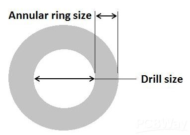
In a multilayer PCB, traces are routed from one layer to another layer with the help of vias. These vias are the holes drilled through copper pads on the surface of the PCB. The amount of copper left around the via on both top and bottom sides of the PCB is called the annular ring.
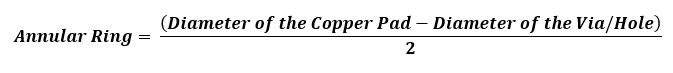
Mathematically, an annular ring is the difference between the diameter of the hole and diameter of the pad divided by 2. For instance, if the diameter of the pad is 24 mils and the diameter of the hole is 12 mils then the width of the annular ring is [(24-12)/2] = 6 mils
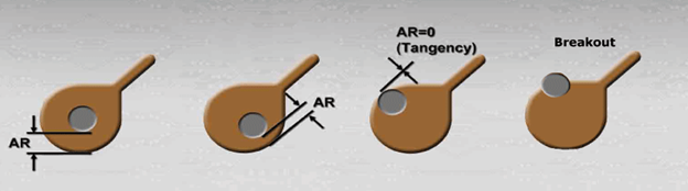
Calculation of the width of an annular ring plays an important role at the time of PCB manufacturing. If the width of the annular ring is not enough then the hole could touch the boundaries of the pad, this condition is called ‘Tangency’. In the extreme situation, the hole could be outside the boundary of the pad which is termed as ‘Breakout’. Both these situations should be avoided during the process of PCB fabrication.

|
