| Sign In | Join Free | My ecer.jp |
|
| Sign In | Join Free | My ecer.jp |
|
| Categories | 10 Layer PCB |
|---|---|
| Brand Name: | WITGAIN PCB |
| Model Number: | PCB000386 |
| Certification: | UL |
| Place of Origin: | China |
| MOQ: | 1pcs/lot |
| Price: | negotiable |
| Payment Terms: | T/T |
| Supply Ability: | 100kpcs/Moth |
| Delivery Time: | 20 days |
| Packaging Details: | Vacuum package in bubble wrap |
| Layer Count: | 10 Layer |
| Application: | Consumer Electronics |
| Solder Mask: | Green Solder Mask |
| Surface Treatment: | Selective Immersion Gold |
| Drilling: | Blind And Buried Holes |
| TG Degree: | TG170 |
| Company Info. |
| Witgain Technology Limited |
| View Contact Details |
| Product List |
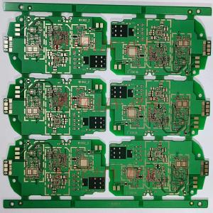
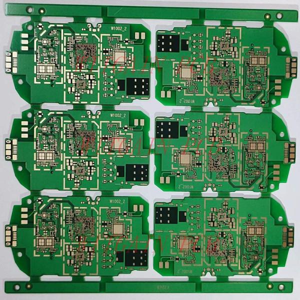
10 Layer Printed Circuit Board ISO 14001 Qualified Used In Medical Equipment
Main Features:
1 10 Layer customized printed circuit board manufacturered based on customer's gerber files.
2 Used in consumer electronics
3 Material is FR4 S1000-2 TG170.
4 The finished board thickness is 1.0MM.
5 The finished copper thickness is 1/H/H/H/H/H/H/H/H/1 OZ.
6 Surface treatment is ENIG 2U'.
7 Drilling: L1-L2 0.1MM, L2-L3 0.1MM, L1-L10 0.2MM, L9-L10 0.1MM, L8-L9 0.1MM Laser Drilling
8 Lead time is around 20 working days.
Material Data Sheet:
| S1000-2 | |||||
| Items | Method | Condition | Unit | Typical Value | |
| Tg | IPC-TM-650 2.4.25 | DSC | ℃ | 180 | |
| IPC-TM-650 2.4.24.4 | DMA | ℃ | 185 | ||
| Td | IPC-TM-650 2.4.24.6 | 5% wt. loss | ℃ | 345 | |
| CTE (Z-axis) | IPC-TM-650 2.4.24 | Before Tg | ppm/℃ | 45 | |
| After Tg | ppm/℃ | 220 | |||
| 50-260℃ | % | 2.8 | |||
| T260 | IPC-TM-650 2.4.24.1 | TMA | min | 60 | |
| T288 | IPC-TM-650 2.4.24.1 | TMA | min | 20 | |
| T300 | IPC-TM-650 2.4.24.1 | TMA | min | 5 | |
| Thermal Stress | IPC-TM-650 2.4.13.1 | 288℃, solder dip | -- | 100S No Delamination | |
| Volume Resistivity | IPC-TM-650 2.5.17.1 | After moisture resistance | MΩ.cm | 2.2 x 10⁸ | |
| E-24/125 | MΩ.cm | 4.5 x 10⁶ | |||
| Surface Resistivity | IPC-TM-650 2.5.17.1 | After moisture resistance | MΩ | 7.9 x 10⁷ | |
| E-24/125 | MΩ | 1.7 x 10⁶ | |||
| Arc Resistance | IPC-TM-650 2.5.1 | D-48/50+D-4/23 | s | 100 | |
| Dielectric Breakdown | IPC-TM-650 2.5.6 | D-48/50+D-4/23 | kV | 63 | |
| Dissipation Constant (Dk) | IPC-TM-650 2.5.5.9 | 1MHz | -- | 4.8 | |
| IEC 61189-2-721 | 10GHz | -- | — | ||
| Dissipation Factor (Df) | IPC-TM-650 2.5.5.9 | 1MHz | -- | 0.013 | |
| IEC 61189-2-721 | 10GHz | -- | — | ||
| Peel Strength (1Oz HTE copper foil) | IPC-TM-650 2.4.8 | A | N/mm | — | |
| After thermal Stress 288℃,10s | N/mm | 1.38 | |||
| 125℃ | N/mm | 1.07 | |||
| Flexural Strength | LW | IPC-TM-650 2.4.4 | A | MPa | 562 |
| CW | IPC-TM-650 2.4.4 | A | MPa | 518 | |
| Water Absorption | IPC-TM-650 2.6.2.1 | E-1/105+D-24/23 | % | 0.1 | |
| CTI | IEC60112 | A | Rating | PLC 3 | |
| Flammability | UL94 | C-48/23/50 | Rating | V-0 | |
| E-24/125 | Rating | V-0 | |||
FQA:
Q1: What is Halogen-Free Solder Paste?
A1: Halogen-Free Solder Paste as the name suggests is a solder paste that does not contain Halogen. Fundamentally, halogens in solder paste refer to chlorine and bromine. Chlorine, is found in circuit boards, and is primarily in the form of residual materials left over from production of non-brominated epoxy resins used in board assembly. Bromine in electronics is usually added to organic materials such as a fire retardant known as brominated flame retardants (BFRs). In solder pastes bromide also play a significant role as activators. Activators are the chemicals that are added to solder fluxes to remove oxides from metal surfaces, and so allow them to join together to form a strong metallurgical bond.
Over last few years the electronics industry has been making a move to become "halogen-free" as this is more environmentally friendly. According to the JPCA-ES-01–2003, IEC 614249–2–21 and IPC 4101B standards set by industry bodies the limit for assembly halogen content is 900 ppm for, chlorine and bromine. The IEC and IPC standard bodies have set the limit for the total, combined amount of chlorine and bromine to be less than 1500 ppm.
Halogens considerably influence the wetting properties of solder paste. Halogens in solder pastes enable solder and solder pad deoxidation, which in turn boost the wetting properties of the solder paste thus improving its melting properties. Hence, they have a positive effect on the stencil life, thermal stability, the reflow process-window, as well as durability. The abandonment of halogens has a direct effect on the soldering process and other subsequent processes such as assembly cleaning. There can always be chances of poorly wetted solder joints while using halogen-free solder pastes. Also, the elimination of halogens as activators can result in head-in-pillow joints due to poor/inconsistent melting behaviour.
So, despite being an essential part of PCB world, why are halogens of concern?
There are both known and suspected risks associated with halogens in electronics. Since various halogens contained in solder pastes, are regarded as harmful to health and the environment, REACH and RoHS have banned the use of halogens. The main concern here is with the disposal of products containing halogens, particularly through incineration as a recovery method. Limits for halogens or halides are set by a number of industrial standards.
The primary replacements for BFRs (Brominated flame retardants) are phosphorous-based materials. Such constituents are typically more hydrophilic, hence, significantly more halogen-free material is required to achieve the same level of flammability resistance. However, aftereffects of using these materials include shorter shelf life, greater PCB stiffness, and lower coefficient of thermal expansion (CTE). On the other hand, halogen-free pastes often have greater thermal stability than traditional FR-4 substrates.
Halide-free fluxes are classically less active than the halogenated pastes. And as result, many of them do not wet as well and have a greater negative effect on joint quality. In the world of solder pastes and fluxes, we typically use the term "halide-free”. So, whether halogen-free and halide-free are synonymous and if not, then what is the difference between a halogen and a halide.
Are Halogen-Free and Halide-Free the same? What is the difference between halogens and halides?
The term halogen refers to any element in the Group 17 of the periodic table, that includes elements like Cl, Br, Fl (Fluorine), I (iodine), and At (Astatine). Therefore, halogen-free technically means "no F, Cl, Br, I, or At. A halide on the other hand is a chemical compound that contains a halogen. For example, table salt (NaCl) is a halide. J-STD 004 categorizes the halide content of solder pastes and thus the corrosion potential of flux residues after soldering. The categories used in denoting the halide content are L (low), M (medium), and H (high). Additionally, 0 and 1 are assigned for halide content (0 = halide-free or below 0.05 % mass fraction halide content, 1 = contains halides).
According to J-STD-004 a flux can be characterized as halide-free if it contains less than a 0.05 % mass fraction of ionic halogen compounds. The same flux might contain some other halogen compounds such as organic acids with chlorine and/or bromine as activators. Hence, it is not necessarily halogen-free according to IEC 61249–2–21. Therefore, in this context, halide-free is not synonymous with halogen-free.
|