| Sign In | Join Free | My ecer.jp |
|
| Sign In | Join Free | My ecer.jp |
|
| Categories | Electronics PCB Design |
|---|---|
| Brand Name: | YDY |
| Model Number: | P-013 |
| Certification: | ISO13485, IATF16949, ISO9001 |
| Place of Origin: | China |
| MOQ: | 1pcs |
| Price: | Negotiatable |
| Payment Terms: | L/C, D/A, D/P, T/T, Western Union, MoneyGram |
| Supply Ability: | 100000/month |
| Delivery Time: | 1-5 working days |
| Packaging Details: | Anti-static bag + white pearl cotton (used around the inside of the carton) + carton |
| Name: | 1-18Layers High Speed Digital Electronics PCB Design Single/Double PCBA |
| Min. line width: | 0.1 0mm |
| Surface finishing: | ENIG,OSP |
| Copper thickness: | 1~2oz |
| Item: | DGW-1 |
| Application: | prototype PCB |
| Color: | Green/Blue/Red/White/Yellow/Black |
| Base material: | Copper Core |
1-18Layers High Speed Digital Electronics PCB Design Single/Double PCBA
We provide one-stop PCB/PCBA customization services:
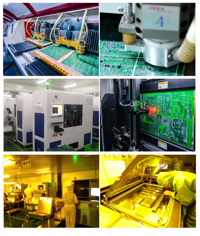
1. To offer good quality PCB/PCBA to our customer, we will do many
kind of testing to ensure quality before shipment
2. Outgoing test to check min PTH Cu thickness, Min surface Cu
thickness, ENIG Au data,Ni data, Au layer adhesion testing,
soldermask adhesion testing, silkscreen adhesion testing, Thermal
stress testing, hardness testing, Twist testing, Bow testing
3. Microsection testing to check hole Cu thickness, Surface Copper
thickness, Wrap copper thickness, Hole Wall Integrity, soldermask
thickness and stack up.
4. E-test to check any open/short circuit.
5. Thermal Stress Test to avoid any Delamination, Measling and
others.
6. Solderability of PTH to avoid any discolor, Wrinkles, Blisters,
Measling, Blow-Hole, Solermask peel off, and soldermask filled in
hole-wall incompletely.
PCB capability:
| Item | Specification | |
| 1 | Numbr of Layer | 1-18Layers |
| 2 | Material | FR-4,FR2.Taconic,Rogers, CEM-1 CEM-3,ceramic , crockery Metal-backed Laminate |
| 3 | Surface Finish | HASL(LF), Gold plating, Electroless nickel immersion gold, Immersion Tin, OSP(Entek) |
| 4 | Finish Board Thickness | 0.2mm-6.00 mm(8mil-126mil) |
| 5 | Copper Thickness | 1/2 oz min;12 oz max |
| 6 | Solder Mask | Green/Black/White/Red/Blue/Yellow |
| 7 | Min.Trace Width & Line Spacing | 0.075mm/0.1mm(3mil/4mil) |
| 8 | Min.Hole Diameter for CNC Driling | 0.1mm(4mil) |
| 9 | Min.Hole Diameter for punching | 0.9mm(35mil) |
| 10 | Biggest panel size | 610mm*508mm |
| 11 | Hole Positon | +/-0.075mm(3mil) CNC Driling |
| 12 | Conductor Width(W) | 0.05mm(2mil)or; +/-20% of original artwork |
| 13 | Hole Diameter(H) | PTH L:+/-0.075mm(3mil); Non-PTH L:+/-0.05mm(2mil) |
| 14 | Outline Tolerance | 0.125mm(5mil) CNC Routing; +/-0.15mm(6mil) by Punching |
| 15 | Warp & Twist | 0.70% |
| 16 | Insulation Resistance | 10Kohm-20Mohm |
| 17 | Conductivity | <50ohm |
| 18 | Test Voltage | 10-300V |
| 19 | Panel Size | 110×100mm(min);660×600mm(max) |
| 20 | Layer-layer misregistration | 4 layers:0.15mm(6mil)max; 6 layers:0.25mm(10mil)max |
| 21 | Min.spacing between hole edge to circuity pqttern of an inner layer | 0.25mm(10mil) |
| 22 | Min.spacing between board oulineto circuitry pattern of an inner layer | 0.25mm(10mil) |
| 23 | Board thickness tolerance | 4 layers:+/-0.13mm(5mil); 6 layers:+/-0.15mm(6mil) |
| 24 | Impedance Control | +/-10% |
| 25 | Different Impendance | +-/10% |
We form close working relationships between Electronics Engineers, Designers, Bare Board Manufacturers, and together with our own in house Test and Assembly facilities. Identify problem areas before they become an issue. Make recommendations that could possibly increase manufacturing or assembly yields on volume product.This approach shortens the design cycle, reducing the time to market, which in turn reduces the overall cost of a project, leading to a more cost effective product.
If you don't have a circuit or any PCB data. We can reverse engineer most bare PCB’s and provide you with up to date schematic diagrams and PCB design data.
Shenzhen Yideyi Technology Co., Ltd is an advanced technology company specialized in researching & developing, designing and manufacturing all types of intelligent control panels and controllers. We implement electronic product designs, industrial system automation designs, electronic circuit hardware and software designs and others while fulfilling OEM/ODM purchase orders. Our main focus is on R&D and technically-driven electronics manufacturing services (EMS).
FAQ:
Q1. How can we ensure our information should not let third party to see o

|
