| Sign In | Join Free | My ecer.jp |
|
| Sign In | Join Free | My ecer.jp |
|
| Categories | SMT PCBA |
|---|---|
| Brand Name: | YDY |
| Model Number: | M-012 |
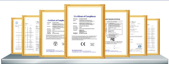
| Certification: | ISO13485, IATF16949, ISO9001,IOS14001 |
| Place of Origin: | China |
| MOQ: | 1pcs |
| Price: | Negotiable |
| Payment Terms: | L/C, D/A, D/P, T/T, Western Union, MoneyGram |
| Supply Ability: | 50000pcs/month |
| Delivery Time: | 1-20 working days |
| Packaging Details: | Vacuum packing or Anti-static package,Outer:export carton or according to the customer's requirement. |
| Service: | SMT PCBA |
| Type: | Square Printed Circuit Design & Fab Circuits Assembly SMT PCBA |
| Copper thickness: | 1oz,0.5-2.0 oz,1oz~3oz,0.5-5 oz, |
| Surface finishing: | HASL,OSP,ENIG,HASL Lead Free,immersion gold |
| Ionic Contamination: | <1.56ug/cm2(NaCl) |
| Peel Strength: | ≥1.4N/mm |
| Drill Hole Diameter: | 0.005"-0.255" (0.15mm~6.5mm) |
| Surface: | HASL Lf/Enig/OSP |
Square Printed Circuit Design & Fab Circuits Assembly SMT PCBA
Shenzhen Yideyi Technology Co., Ltd is a professional PCBA solution service provider specializing in one-stop service from PCB, components purchasing, PCB fabrication, pcba clone,SMT PCB assembly to complete products building.
Our products are widely used in meter, medical, solar energy, mobile, communication, industrial control, power electronics,security, consuming, computer, automotive, aerospace, military and so on. Over 75% of our products are exported to Europe, North America, Japan and other Asia Pacific countries. Based on many years of development, we have high-qualified management team, experienced R&D team and skilled employees,and possess advantaged supply chain, commitment to quality,and dedication to our customers service.
Encouraging innovation and keeping improving. Besides achieving corporate and customer values, we also create a favorable atmosphere for employees to achieve personal values. Endeavor to provide every member with broad space for individual goals. "Science and technology innovation win-win world,We provide the best products and services."
We have high-qualified management team, experienced R and D team and skilled employees and possess advantaged supply chain, commitment to quality and dedication to our customers service
All our products follow IPC class and are approved by UL, RoHS and ISO9001. Also our executives and technicians are experienced people who have been engaged in PCB industry for more than twenty years so we have rich production management experience and professional PCB skills. We ensure the quality of PCB products by continuously introducing new equipment′s and new technologies and using high quality materials. With professional technicians we can provide early design consultation and technical support, so that customers can be more worry-free. With qualified and reliable products, advanced technology and value-added service, we won the trusts and supports of customers and established a good reputation in the industry.
SMT PCBA capabilities:
• SMT assembly including BGA assembly
• Accepted SMD chips: 01005,BGA,QFP,QFN,TSOP
• Component height: 0.2-25mm
• Min packing: 0201
• Min distance among BGA : 0.25-2.0mm
• Min BGA size: 0.1-0.63mm
• Min QFP space: 0.35mm
• Min assembly size: (X*Y): 50*30mm
• Max assembly size: (X*Y): 350*550mm
• Pick-placement precision: ±0.01mm
• Placement capability: 0805, 0603, 0402, 0201
• High pin count press fit available
• SMT capacity per day: 800,000 point
Advantages:
• Strict product liability, taking IPC-A-160 standard
• Engineering pretreatment before production
• Production process control (5Ms)
• 100% E-test, 100% visual inspection, including IQC, IPQC, FQC, OQC
• 100% AOI inspection, including X-ray, 3D microscope and ICT
• High-voltage test, impedance control test
• Micro section, soldering capacity, thermal stress test, shocking test
• In-house PCB production
• No minimum order quantity and free sample
• Focus on low to medium volume production
• Quick and on-time delivery
Our goal is to be the leading PCB solutions provider in the electronics industry with first-class products and services. We are devoted to be a trusted partner of our customers.
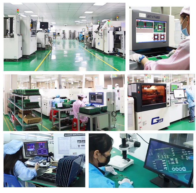
Production processes:
Material Receiving → IQC → Stock → Material to SMT → SMT Line Loading → Solder Paste/Glue Printing → Chip Mount → Reflow → 100% Visual Inspection → Automated Optical Inspection (AOI) → SMT QC Sampling → SMT Stock →
Material to PTH → PTH Line Loading → Plated Through Hole → Wave Soldering → Touch Up → 100% Visual Inspection → PTH QC Sampling → In-Circuit Test (ICT) → Final Assembly → Functional Test (FCT) → Packing → OQC Sampling → Shipping
PCB assembly Equipment:
1. High speed and precision chip placer or multi-function SMD mounter
2. Wave soldering machine
3. Vacuum machine
4. High temperature box
5. Auto-solder paste printer
6. Hot- and mixed-air reflow
Each board is carefully examined by our dedicated inspection team using AOI and high magnification viewers.
Using our X-Ray machine, we test PCBs to component level and all wiring is fully inspected and tested. Flash
testing and earth bonding tests can also be undertaken where required.
SMT PCBA Manufacture Capacity
| Process | Item | Mass production capability | |
| SMT | Printing | Max PCB size | 900*600mm² |
| Max PCB weight | 8kg | ||
| Solder paste printing tolerance | ±25μm(6σ) | ||
| System repeat calibration tolerance | ±10μm(6σ) | ||
| Scraper pressure detection | pressure closed-loop control system | ||
| SPI | Detect Min BGA PAD to PAD distance | 100μm | |
| x-axis and Y-axis tolerance | 0.5μm | ||
| False Rate | ≤0.1% | ||
| Mount | Component size | 0.3*0.15 mm²--200*125 mm² | |
| Component max height | 25.4mm | ||
| Populate Max component weight | 100g | ||
| BGA/CSP Min PAD spacing, and Min PAD diameter | 0.30mm,0.15mm | ||
| Populate tolerance | ±22μm(3σ),±0.05°(3σ) | ||
| PCB board size | 50*50 mm²-850*560 mm² | ||
| PCB thickness | 0.3mm--6mm | ||
| Max PCB weight | 6kg | ||
| Populate Max components type | 500 | ||
| AOI | Detect Min components | 01005 | |
| Detect false type | Incorrect conponents,missing components,opposite direction,,component shift,Tombstone,Mounting on side,unsoldering,insufficient solder,Lead raised,Solder ball | ||
| Foot warping detection | 3D Detection function | ||
| Reflow | Temperature Accuracy | ±1ºC | |
| Welding protection | nitrogen protection;(remaining oxygen<3000ppm) | ||
| Nitrogen Control | Nitrogen closed-loop control system,±200ppm | ||
| 3D X-Ray | Magnification | Geometric Magnification;:2000 times;System Magnification:12000times | |
| Resolution | 1μm /nm | ||
| Rotation Angle &Slanting Perspective | Any ±45°+360°rotation | ||
| DIP | Preelaboration | Automatic forming technology | Component Automatic forming |
| DIP | DIP technology | Automatic Insertion machine | |
| Wave soldering | Wave soldering type | Ordinary wave soldering | |
| Inclination angle of transport guide rail | 4--7° | ||
| Temperature accuracy | ±3ºC | ||
| Soldering protection | nitrogen protection | ||
| Non-welding pressure contact technology | Max PCB board size | 800*600mm² | |
| Press down height accuracy | ±0.02mm | ||
| Pressure Range | 0-50KN | ||
| Pressure Accuracy | Standard value:±2% | ||
| Hold time | 0-9.999S | ||
| Conformal coating technology | Max PCB board size | 500*475*6mm | |
| Max PCB board weight | 5kg | ||
| Min Nozzle size | 2mm | ||
| Other characteristic | Conformal coating pressure Programmable control | ||
| ICT test | test level | Device level test,Test hardware connection status. | |
| Test point | >4096 | ||
| Test content | Contact test ,Open/short test,Resistance capacitance test test,diode, triode,mosfet test,No power on hybrid test,Boundary scan chain test,Power on mixed mode test. | ||
| Assembly and test | Production type | TouchPad | Mass production |
| TWS | Mass production | ||
| Baby Camera | Mass production | ||
| Gaming controller | Mass production | ||
| Life Watch | Mass production | ||
| FT test | test level | PCB board system level test.Test System function status. | |
| Temperature cycling test | Temperature range | -60ºC--125ºC | |
| Rise/lower temperature rate | >10ºC/min | ||
| Temperature tolerance | ≤2ºC | ||
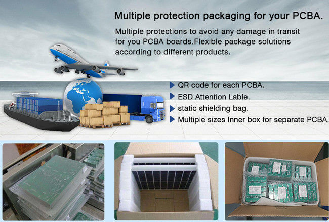
Package &Shipping Methods:
1. Vacuum package with silica gel, Carton box with packing belt.
2. By DHL, UPS, FedEx, TNT
3. By EMS
4. By sea for mass quantity according to customer's requirement
We provide high quality manufacturing services at a competitive price:
FAQ:
Q1. How to keep our product information and design file secret ?
We are willing to sign a NDA effect by customers side local law and
promising to keep customers data in high confidential level.
Q2. What file formats do you accept for production?
Gerber file: CAM350 RS274X
PCB file: Protel 99SE, P-CAD 2001 PCB
BOM: Excel (PDF,word,txt)
Q3. Please note that the following detail will speed up evaluation:
Material:
Board thickness:
Copper thickness:Surface finish:
Solder mask color:
Silkscreen color:
Q4. How to make sure the PCBAs are completely well recieved?
We will pack with aluminum bag, and insert card, up and bottom card
with stable cartons.
Q5. How to ship the PCBAs?
For small packages, we will ship the boards to you by
DHL,UPS,FEDEX,TNT. Door to door service! For mass production, we
could ship by air, by sea.
Q6. How to make sure the function is fine?
We could make sample/prototype and do functional testing before
mass production.
Q7. What Trade Terms do you accept?
Payment: T/T in advance (Western Union , paypal is welcomed)

|
