| Sign In | Join Free | My ecer.jp |
|
| Sign In | Join Free | My ecer.jp |
|
| Categories | PCB Reverse Engineering |
|---|---|
| Brand Name: | YDY |
| Model Number: | M-006 |
| Certification: | ISO13485, IATF16949, ISO9001,IOS14001 |
| Place of Origin: | China |
| MOQ: | 1pcs |
| Price: | Negotiable |
| Payment Terms: | L/C, D/A, D/P, T/T, Western Union, MoneyGram |
| Supply Ability: | 50000pcs/month |
| Delivery Time: | 1-20 working days |
| Packaging Details: | Vacuum packing or Anti-static package,Outer:export carton or according to the customer's requirement. |
| Service: | PCB Reverse Engineering |
| Type: | 1oz IOS14001 Daughter Board Backplane PCB Reverse Engineering |
| Copper thickness: | 1oz,0.5-2.0 oz,1oz~3oz,0.5-5 oz,0.5oz-4oz |
| Ionic Contamination: | <1.56ug/cm2(NaCl) |
| Usage: | OEM Electronics |
| Metal Coating: | (Lead Free) HASL, Immersion Tin&Lgold&Silver etc |
| Test Voltage: | 50-300V |
| Base material: | FR4 CEM1 CEM3 Ceramic Aluminum |
1oz IOS14001 Daughter Board Backplane PCB Reverse Engineering
Shenzhen Yideyi Technology Co., Ltd is a professional PCB manufacturer, which is located in Shenzhen, China. After many years development, it has become a company which integrates research & development, reverse engineering,manufacture, SMT and sales.
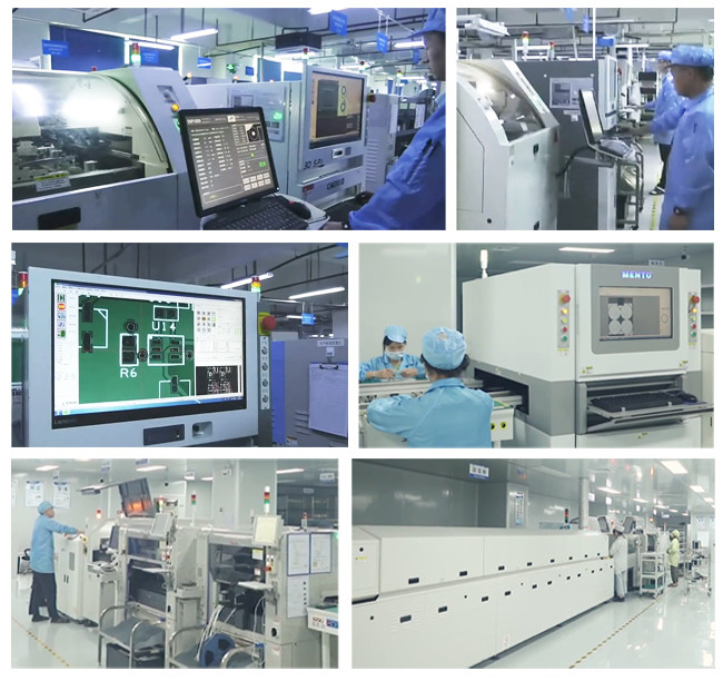
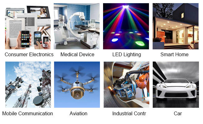
We have served many well-known OEM customer who focuses on marketing and designing. Our products are mainly applied in the consumption, security and safety, industrial, medical, Network, automation, measurement, counter device and other fields. With years of experience, we have gained a good reputation among clients in the electronic production field for reasonable prices, rich resources and punctual delivery.Our manufacturing facilities include clean workshops and advanced high-speed SMT lines. Our chip placement precision can reach +0.1MM on integrated circuit parts. It means we can deal with almost all kinds of integrated circuits, such as SO, SOP, SOJ, TSOP, TSSOP, QFP, BGA and U-BGA. Additionally, we can provide 0201 chip placement, through-hole component insertion and finished product fabrication, test and packing.
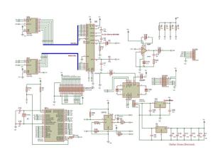
PCB reverse engineering is a reverse research technology that uses a series of reverse research techniques to obtain a PCB design, circuit schematic and a BOM for an existing & matual electronic design.
How PCB Reverse Engineering Would Help PCB Design & Development?
PCB reverse engineering is a reverse research technology that uses a series of reverse research techniques to obtain a PCB design, circuit schematic and a BOM for an existing & matual electronic design. A new product development that used to take two or three years to develop, now through reverse engineering technolgy, may take only a few months to complete.
Why Use Our PCB Reverse Engineering Service?
Our Reverse Engineering Services are designed + developed in accordance with what you want and need. These services are widely appreciated by our clients for their timely execution and genuine prices.
1. Manufactured items are frequently smaller + more efficient — saving you space, time, + costs.
2. All reverse engineering projects use only modern + current components making any future repairs they may need easier + cost effective.
3. Most units are upgradeable — we can add functionality, outputs, sensors, or change programs slightly to broaden your processing capability and to improve operations, maintenance + support issues on older circuit Boards
4. Migration from through hole parts to SMD (Surface Mount Device) parts
5. Migration to emerging technologies while retaining the core features and logic of existing systems
6. Discover product strengths, weaknesses and limitations
7. To understand competitor's products and develop alternatives
8. Manufacturer of a product no longer exists or produces a product
9. Manufacturer of a product no longer supports/services a product
10. Documentation of the original design is lost or inadequate
11. To update obsolete components with current technology
12. Create better designs
PCB Reverse Engineering Services
We will reverse engineer your PCB sample, and submit the engineering file into:
PCB Gerber File
BOM List
Schematic Diagram
YDY service:
1. PCBA, PCB assembly: SMT & PTH & BGA
2. PCBA and enclosure design
3. Components sourcing and purchasing
4. Quick prototyping
5. Plastic injection molding
6. Metal sheet stamping
7. Final assembly
8. Test: AOI, In-Circuit Test (ICT), Functional Test (FCT)
9. Custom clearance for material importing and product exporting
10. PCBA reverse engineering
11. Professtional R&D team
12. PCB Layout Design
Files Requested For Quote:
In order to provide you with the most efficient and accurate quote on manufacturing the requested unit, we ask that you provide us with the following information:
1. Gerber file,PCB file,Eagle file or CAD file are all acceptable
2. A detailed bill of materials (BOM)
3. Clear pictures of PCB or PCBA sample for us
4. Quantity and delivery required
5. Test method for PCBA to guarantee 100% good quality products.
6. Schematics file for PCB design if need to do function test.
7. A sample if available for better sourcing
8. CAD files for enclosure manufacturing if required
9. A complete wiring and assembly drawing showing any special assembly instructions if required
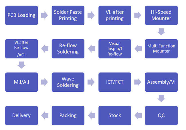
PCB Assembly Manufacturing Procedures:
Program Management
PCB Files → DCC → Program Organizing → Optimization → Checking
SMT Management
PCB Loader → Screen Printer → Checking → SMD Placement → Checking → Air Reflow → Vision Inspection → AOI → Keeping
PCBA Management
THT→Soldering Wave (Manual Welding) → Vision Inspection → ICT → Flash → FCT → Checking → Package → Shipment
Each board is carefully examined by our dedicated inspection team using AOI and high magnification viewers.
Using our X-Ray machine, we test PCBs to component level and all wiring is fully inspected and tested. Flash
testing and earth bonding tests can also be undertaken where required
PCB SMT Manufacture Capacity
| No | Items | Capability |
| 1 | PCB Layers | 2 ~ 15 layers |
| 2 | PCB Base Material | FR4, High Tg FR4, Halogen Free, Isola, Rogers, Aluminium |
| 3 | PCB Finished Board Thickness | 0.2mm ~ 7.0mm(8mil-276mil) |
| 4 | PCB Copper Thickness | 1/3oz ~ 7oz |
| 5 | PCB Surface Finishing | HASL, Lead Free HASL, Immersion tin, Immersion gold, Gold plating, Immersion silver, OSP, Carbon, etc. |
| 6 | PCB Max gold plating thickness | 50 microinch |
| 7 | PCB Min. Trace Width/Space | 0.075/0.075mm(3/3mil) |
| 8 | PCB Min. Finish Holes Size | 0.1mm(4mil) for laser holes; 0.2mm(8mil) for mechanical holes |
| 9 | PCB Max. Finshed Size | 600mm X 900mm (23.6" X 35.43") |
| 10 | PCB Hole Tolerance | PTH: ±0.076mm(+/-3mil), NTPH: ±0.05mm(+/-2mil) |
| 11 | PCB Soldermask Color | Green, White, Black, Red, Yellow, Blue, |
| 12 | PCB Silkscreen Color | White, Black, Yellow, Blue |
| 13 | PCB Impedance Control | +/-10% |
| 14 | PCB Profiling Punching | Routing, V-CUT, Chamfer |
| 15 | PCB Special Holes | Blind/Buried holes, Countersunk holes |
| 16 | PCB Reference Standard | IPC-A-600H Class 2, Class 3, TS16949 |
| 17 | PCB Certificate | UL, ISO9001, RoHS, SGS |
| 18 | PCB Package | Vacuum & Carton |
We can reverse engineer any industry PCBA for you:
FAQ:
Q1. How to keep our product information and design file secret ?
We are willing to sign a NDA effect by customers side local law and
promising to keep customers data in high confidential level.
Q2. How long does it take for PCB and PCBA Quote ?
PCBs quotation within 2 hours can finished the PCBA depend on the
components
quantity,if simple, within 6 hours can finished,once complex and
more,the 12- 36 hours
can be finished.
Q3. Please note that the following detail will speed up evaluation:
Material:
Board thickness:
Copper thickness:Surface finish:
Solder mask color:
Silkscreen color:
Q4. How to make sure the PCBAs are completely well recieved?
We will pack with aluminum bag, and insert card, up and bottom card
with stable cartons.
Q5. How to ship the PCBAs?
For small packages, we will ship the boards to you by
DHL,UPS,FEDEX,TNT. Door to door service! For mass production, we
could ship by air, by sea.
Q6. How to make sure the function is fine?
We could make sample/prototype and do functional testing before
mass production.

|