| Sign In | Join Free | My ecer.jp |
|
| Sign In | Join Free | My ecer.jp |
|
| Categories | Rapid PCBA |
|---|---|
| Brand Name: | HNL-PCBA |
| Model Number: | PCB Assembly |
| Certification: | ISO9001:2015 ,UL 94V0 ,ROHS |
| Place of Origin: | CHINA |
| MOQ: | 1 PC |
| Price: | Negotiable |
| Payment Terms: | T/T, Western Union, L/C, MoneyGram |
| Supply Ability: | 10,000,000 Point /Day |
| Delivery Time: | 1-7days |
| Packaging Details: | ESD packaging with carton box |
| Product name: | AOI Pcba |
| Copper thickness: | 1/3oz-6oz |
| Min. line spacing / Width: | 0.030mm /0.030mm |
| Board thickness: | 0.3mm-3.5mm |
| Min. hole size: | Laser 0.05mm ; Mechnical 0.15 |
| Surface treatment: | OSP,HAL,HAL LF,ENIG,Hard gold,Imm Ag,Imm Sn,Peelable soldermask,Carbon ink print,Selective hard gold |
| Base material: | High Tg FR-4, Halogen Free FR-4, Thick Copper FR-4, Aluminium Based, Rogers, Taconic |
| Application: | Medical Equipments, Consumer Electronics ,automotive Electronics Etc. |
| Solder mask color: | Green,white,black,red,orange,yellow,blue,purple |
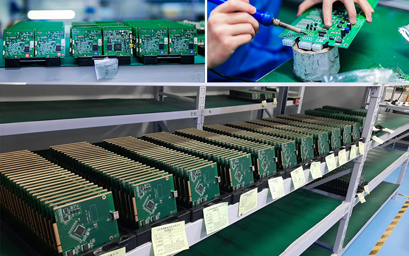
PCBA can be understood as a finished circuit board. The essence is PCB and component assembly. PCB is a printed circuit board and a support for electronic components. PCB procurement and patch processing are two different production methods.
PCBA is the abbreviation of Printed Circuit Board Assembly in
English, that is to say, PCB blank board goes through SMT loading,
or the entire process of DIP plug-in, referred to as PCBA, and the
standard way of writing in Europe and America is PCB'A, with "'"
added, this Known as the official idiom.
| FACTORY CAPABILITIES | |||
| No. | Items | 2019 | 2020 |
| 1 | HDI Capabilities | HDI ELIC (4+2+4) | HDI ELIC(5+2+5) |
| 2 | Max layer count | 32L | 36L |
| 3 | Board Thickness | Core thickness 0.05mm-1.5mm ,Fineshed board thickness 0.3-3.5mm | Core thickness 0.05mm-1.5mm ,Fineshed board thickness 0.3-3.5mm |
| 4 | Min.Hole Size | Laser 0.075mm Mechnical 0.15 | Laser 0.05mm Mechnical 0.15 |
| 5 | Min Line Width/Space | 0.035mm/0.035 | 0.030mm/0.030mm |
| 6 | Copper Thickness | 1/3oz-4oz | 1/3oz-6oz |
| 7 | Size Max Panel size | 700x610mm | 700x610mm |
| 8 | Registration Accuracy | +/-0.05mm | +/-0.05mm |
| 9 | Routing Accuracy | +/-0.075mm | +/-0.05mm |
| 10 | Min.BGA PAD | 0.15mm | 0.125mm |
| 11 | Max Aspect Ratio | 10:1 | 10:1 |
| 12 | Bow and Twist | 0.50% | 0.50% |
| 13 | Impedance Control Tolerance | +/-8% | +/-5% |
| 14 | Daily output | 3,000m2 (Max capacity of equipment) | 4,000m2 (Max capacity of equipment) |
| 15 | Surface Finishing | HASL Lead Free /ENEPING /ENIG /HASL /FINGER GOLD/IMMERSION TIN/SELECTIVE THICK GOLD | |
| 16 | Raw Material | FR-4/Normal Tg/High Tg/Low Dk/HF FR4/PTEE/PI | |
| PCBA Capability | |||
| Material Type | Item | Min | Max |
| PCB | Dimension (length,width,height.mm) | 50*40*0.38 | 600*400*4.2 |
| Material | FR-4,CEM-1,CEM-3,Aluminium-based board,Rogers,ceramic plate,FPC | ||
| Surface finish | HASL,OSP,Immersion gold,Flash Gold Finger | ||
| Components | Chip&IC | 1005 | 55mm |
| BGA Pitch | 0.3mm | - | |
| QFP Pitch | 0.3mm | - | |
Our service
PCB Design & Layout
PCB Prototyping
PCB Fabrication
Turn Prototype PCB Assembly
PCB Assembly Services
PCB'A
Printed Circuit Board Assembly PCBA
AL-SPI-IA
solder paste printing equipment
wave-soldering
automatic printing equipment
60times magnifying glass
material baking equipment
X-ray welding inspection
Semi-automatic printing equipment
component counting equipment
Online AOI detector
Reflow welding equipment
Mydata welding equipment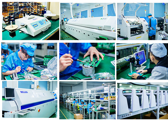
Printed circuit boards And PCB Assembly are mainly used for many
communication industry ,Aprospace ,Auto Industry
,Communication,Indutrial Control ,Medical device ,Smart
Home,consumer electronics ,automotive electronics , audio and
video, optoelectronics, robotics, hydroelectric power, aerospace,
education, power supply, printer ,Auto Industry ,Smart Home.etc.
PCB: Vacuum packaging with carton box
PCBA: ESD packaging with carton box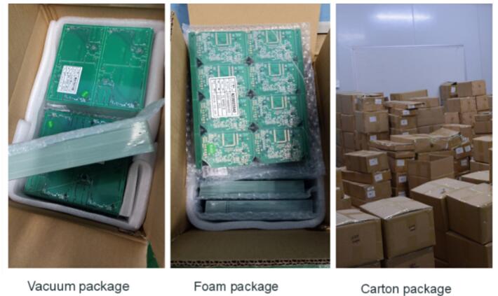
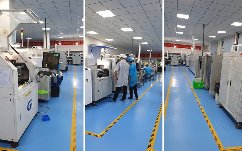
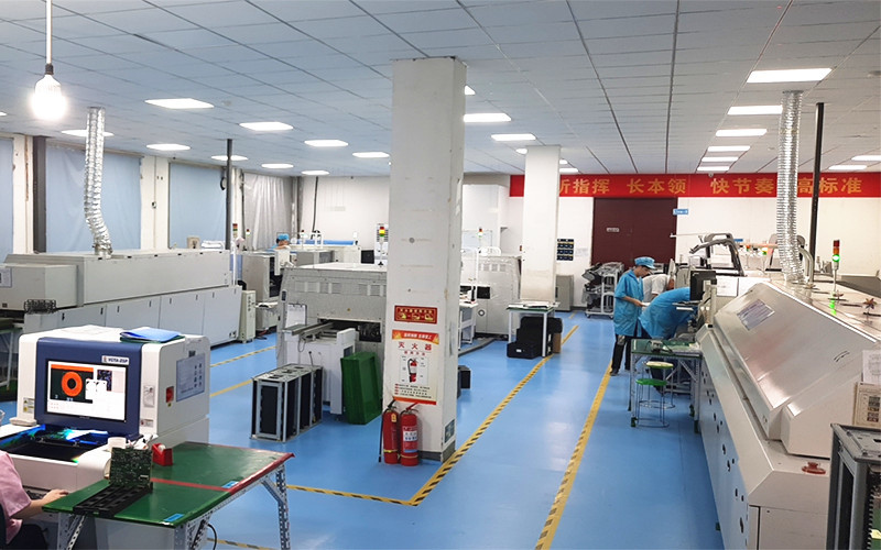
Company Information
Beijing Haina lean Electronics Co.,Ltd is one of the most
professional PCB manufacture in Beijing,China. With more then 10
years of development, Haina Lean Electronics turns into a first
class manufacture of HDI PCB ,with production capability 4000
square meters.
Our factory is providing high quality bare PCB, PCB layout design
service and PCB assembly service,including components sourcing,
function test,conformal coating and complete assembly for clients
all.
We have profuse experience in manufacturing PCB,owned experienced
technical R & D technology team, young and professional sales and
customer service team, experienced and professional procurement
team and assembly testing team, which make sure the products
quality of the pass rate, on-time delivery rate of customer orders.
Our services include: circuit board design and layout, 2-46 layers
PCB manufacturing, professional FPC production, electronic
components purchasing, SMT professional processing, Soldering and
Assembly, especially sample and small bulk orders. we have the
advantages of a quick quote, fast production, fast delivery.
The company pursues "inclusiveness, excellence, people-oriented".
Constantly innovate, take technology as the core, regard quality as
life, and wholeheartedly provide customers with high-quality and
high-efficiency humanized services.We are willing to serve our
customers with the principle of continuous honesty &
trustworthiness, pragmatism and innovation.

|
