| Sign In | Join Free | My ecer.jp |
|
| Sign In | Join Free | My ecer.jp |
|
| Categories | Silicon Wafer |
|---|---|
| Brand Name: | BonTek |
| Model Number: | Silicon Wafer |
| Certification: | ISO:9001, ISO:14001 |
| Place of Origin: | China |
| MOQ: | 25 Pieces |
| Price: | Negotiable |
| Payment Terms: | T/T |
| Supply Ability: | 100000 Pieces/Month |
| Delivery Time: | 1 - 4 weeks |
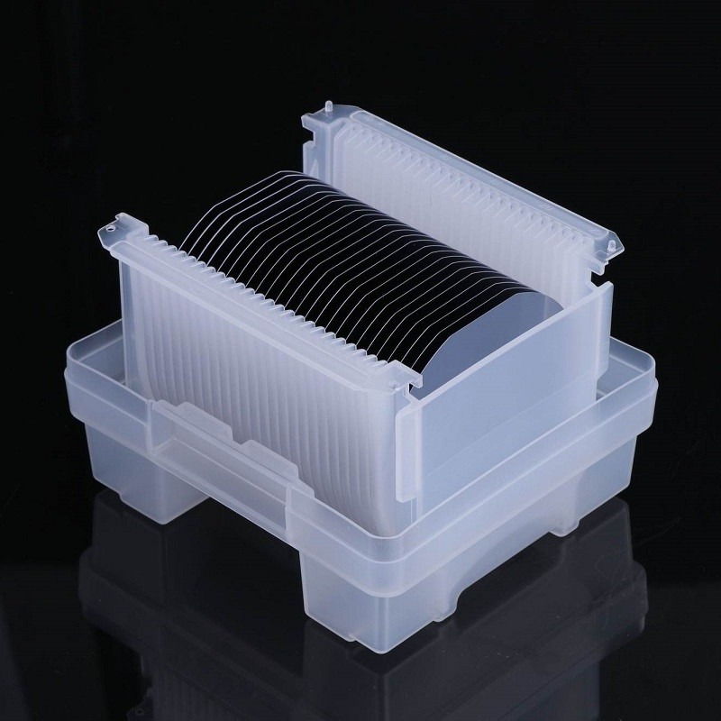
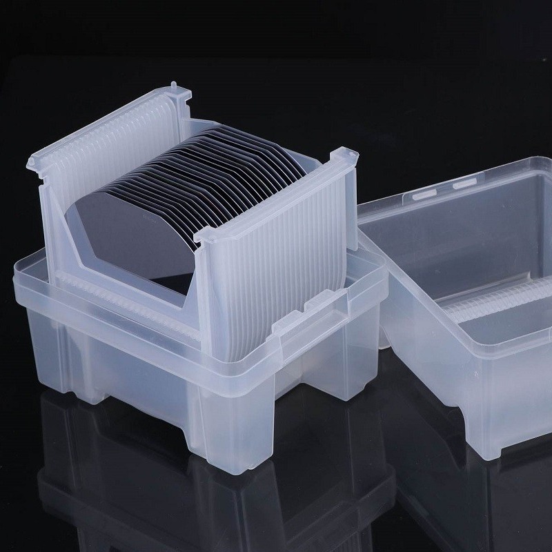
| Packaging Details: | Cassette / Jar, put in a carton with PE foam. |
| Material: | Silicon Wafer |
| Surface: | Double Side Polish, Single Side Polish, Lap |
| Diameter: | 2'' - 12'' or as required |
| Thickness: | 0.05mm - 10mm |
| Orientation: | <100>, <111>, <110> |
| Resistivity: | 0.001 – 300 ohm/cm |
| Type: | P type, N type, Intrinsic |
| Dopant: | B, Ph, As or Undoped |
| Company Info. |
| Hangzhou Freqcontrol Electronic Technology Ltd. |
| Verified Supplier |
| View Contact Details |
| Product List |
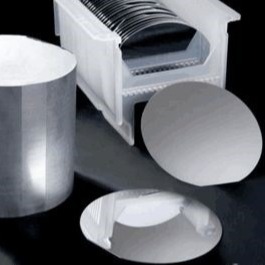
2'' To 12'' P Type N Type Silicon Wafer With High Resistivity for Semiconductor
BonTek produce silicon wafers (12 inches or less) for semiconductors in an integrated manner ranging from single crystal ingots to wafer processing. We have established the supply system mainly for the mass-produced wafers for bipolar integrated circuits, discrete circuits, and MEMS.
Silicon wafers are manufactured by cutting, polishing and cleaning single crystals of high-purity silicon under a strict production and quality control system. Diameter provided 4in, 5in, 6in, 8in, and 12inch.
SEMI Standard | 2" (50.8mm) | 3" (76.2mm) | 4" (100mm) | 5" (125mm) | 6" (150mm) | 8" (200mm) | 12" (300mm) |
|---|---|---|---|---|---|---|---|
Diameter | 50.8 ± 0.38mm | 76.2 ± 0.63mm | 100 ± 0.5mm | 125 ± 0.5mm | 150 ± 0.2mm | 200 ± 0.2mm | 300 ± 0.2mm |
Thickness | 279 ± 25µm | 381 ± 25µm | 525 ± 20 µm or 625 ± 20µm | 625 ± 20µm | 675 ± 20µm or 625 ± 15µm | 725 ± 20µm | 775 ± 20µm |
Type | P, N or Intrinsic | ||||||
Dopant | B, Ph, As or Undoped | ||||||
Orientation | <100>, <111>, <110> | ||||||
Rsistivity | 0.001 – 300 ohm/cm | ||||||
Primary Flat Length | 15.88 ± 1.65mm | 22.22 ± 3.17mm | 32.5 ± 2.5mm | 42.5 ± 2.5mm | 57.5 ± 2.5mm | Notch | Notch |
Secondary Flat Length | 8 ± 1.65mm | 11.18 ± 1.52mm | 18 ± 2.0mm | 27.5 ± 2.5mm | 37.5 ± 2.5mm | NA | NA |
Surface Finish | SSP, DSP, Etched, or Lapped | ||||||
Acceptance Check
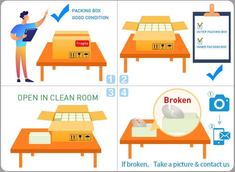
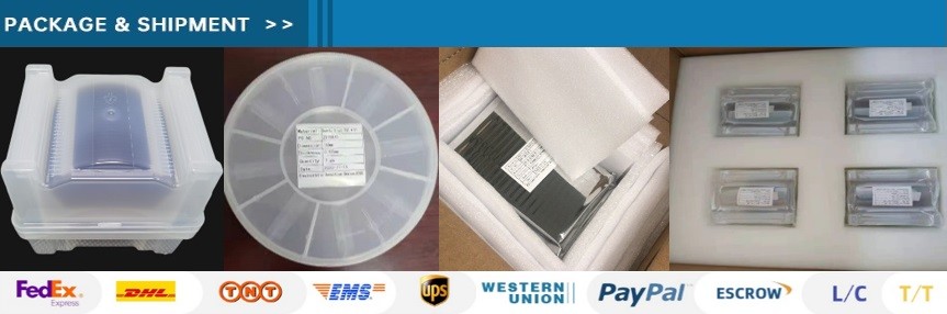
1. The product is fragile. We have adequately packed it and labeled it fragile. We deliver through excellent domestic and international express companies to ensure transportation quality.
2. After receiving the goods, please handle with care and check whether the outer carton is in good condition. Carefully open the outer carton and check whether the packing boxes are in alignment. Take a picture before you take them out.
3. Please open the vacuum package in a clean room when the products are to be applied.
4. If the products are found damaged during courier, please take a picture or record a video immediately. DO NOT take the damaged products out of the packaging box! Contact us immediately and we will solve the problem well.

|
