IBE Electronics Co.,ltd has been serving the contract
manufacturing (ODM,OEM/EMS), industry for 25 years in
China. The service includes Electronic Device Design , PCB
Fabrication, components sourcing, PCB Assembly,conformal coating,
sub-assembly and programming&testing, to final box
packing, a Turnkey Solution. To expand the business and
provide better services to North American customers, IBE
opened new facilities IBE (USA) in 40760 Encyclopedia Cir,Fremont, CA, 94538 in 2017, and IBE(Vietnam) in Dai Dong Industrial Zone-Hoan Son, Hoan Son Commune, Tien Du
District, Bac Ninh Province, which can provide a full range of PCB assembly service. IBE
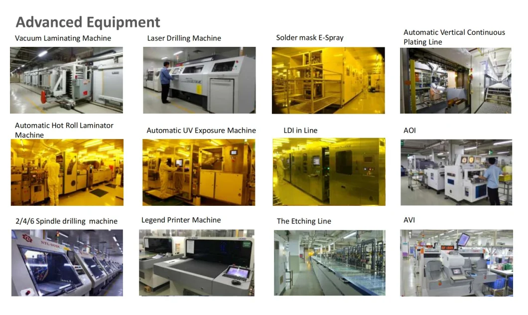
continues to invest in new technologies, providing a complete
manufacturing solution to meet customers' needs and make the
process more economical. Our major products are in markets of
IOT,Smart Metering,Medical Device,Automotive Electronic
Device,Industrial mather board, and laser devices.
Our main customers: BMW, TELSA, EATON, BOSCH, ABB, Honeywell...
Bare PCB capacity: 150000sqm/month
PCB ability:2layers ~28layers
Assembly capacity: 350,000components/hour
Assembly Ability: Min components:0201
Lead time: quick turn: 24hours
Advantage: No MOQ, short lead time, TS16949/ISO14001/ISO13485
qualified process, cost effectiveness
Welcome to make inquiry with Gerber file and Bom lists!