| Sign In | Join Free | My ecer.jp |
|
| Sign In | Join Free | My ecer.jp |
|
| Categories | Printed Circuit Boards |
|---|---|
| Brand Name: | WITGAIN PCB |
| Model Number: | Copper Based PCB005 |
| Certification: | UL |
| Place of Origin: | China |
| MOQ: | 1pcs/lot |
| Price: | negotiable |
| Payment Terms: | T/T |
| Supply Ability: | 100kpcs/Month |
| Delivery Time: | 10 days |
| Packaging Details: | Vacuum package in bubble wrap |
| Layer Count: | 1 Layer |
| PCB Thickness: | 1.8 MM |
| CU Thickness: | 1 OZ |
| Application: | LED Light |
| Lead Time: | 15 days |
| Solder Mask: | White Solder Mask |
| Company Info. |
| Witgain Technology Limited |
| View Contact Details |
| Product List |
3 W/MK Conductivity Copper Substrate Single Layer PCB Used In Led
Specifications:
1 All dimensions are in MM.
2 Fabricate per IPC-6012A Class2.
3 Materials:
3.1 Dielectric: Aluminum
3.2 Min Tg: 150DEG
3.3 Copper: As per stack up
3.4 UL Rating: 94V0 Minimum
4 Surface finish: ENIG 1U
5 Solder mask material should meet all requirement of the
IPC-SM-840E and shall be green in color and applied over bare
copper. Vendor may edit solder mask and paste mask as needed.
6 Editing of existing copper layers shall require customer
approval.
7 Silkscreen legend to be applied per layer stackup using white
non-conductitive epoxy ink.
8 100% continuity testing using database netlist shall be
performed.Vendor to identify test passed in secondary side.
9 Vendor to mark date code and logo in legend secondary side.
10 Bow and twist shall not exceed 1.0% of longest side.
11 Vendor to provide panel drawing for customer approval before
production
PCB report have to include the following information:
1 Measurement: outline dimension, pcb thickness, plating thickness,
actual hole size dimension, copper thickness, hole wall copper
thickness, solder mask thickness, track and space width, warp and
twist percentage;
2 Test and inspection: electrical test result, solder ability test
result, visual inspection test result, micro section pcb with
resin;
3 Other: date code, quantity etc.
FQA:
Q1: What are Copper Based PCBs?
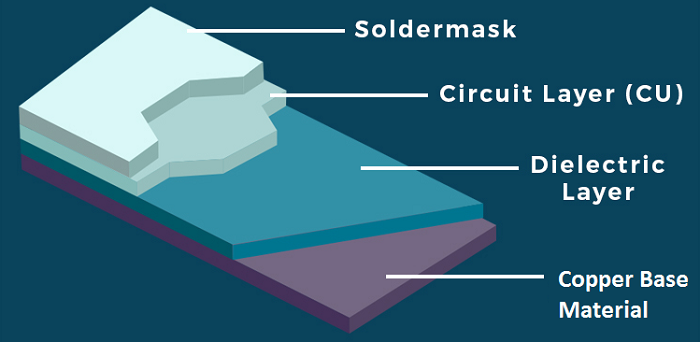
A1: Copper-based PCBs use copper as a primary base material in place of
commonly used FR4. The copper base material is then covered with an
insulating layer followed by a circuit layer. Copper core/based
PCBs are known to have excellent heat dissipation and can be used
for high frequency applications with minimal variation in
performance over wide temperature ranges. However, these advantages
do come at a cost (literally), Cu Core PCB’s are vey expensive.

Advantages of Cu Based PCBs:
Limitations of Cu Based PCBs:

|