| Sign In | Join Free | My ecer.jp |
|
| Sign In | Join Free | My ecer.jp |
|
| Categories | High Frequency PCB |
|---|---|
| Brand Name: | HNL-PCBA |
| Model Number: | PCB Assembly 06 |
| Certification: | ISO9001,IS16949, ISO14001,ROHS , UL, IPC-A ,QC080000 |
| Place of Origin: | CHINA |
| MOQ: | 1 PC |
| Price: | Negotiable |
| Payment Terms: | T/T, Western Union, L/C, MoneyGram |
| Supply Ability: | 10,000,000 Point /Day |
| Delivery Time: | 1-7days |
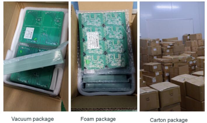
| Packaging Details: | ESD packaging with carton box |
| Product name: | High Frequency PCB |
| Material: | FR-4/HG150-180 |
| Copper thickness: | 1/3OZ to 6OZ |
| Min. line widthng: | 0.030mm |
| Board thickness: | 0.3mm to 3.5mm |
| Min. hole size: | Laser 0.075mm; Mechnical 0.15mm |
| Surface finishing: | HASL,ENIG,HASL Lead Free,OSP,Immersion gold |
| Solder mask: | Green. Red. Blue. White. Black.Yellow |
| PCB Assembly method: | Mixed; SMT, DIP, THT ETC. |
| Usage: | OEM Electronics,Circuit Board Assembly |
Satellite communication growing rapidly, information products move towards high speed and high frequency. Thus developing new products always need to use high frequency substrate, satellite system, mobile telephone receiving base station and so on, these communication products must use high frequency PCB.
produce HDI board, Fast PCB board, RF PCB board, PCBA, high frequencyPCB board ,high speed board and rigid-flex board, etc., to meet customers' various demands.
| FACTORY CAPABILITIES | |||
| No. | Items | 2019 | 2020 |
| 1 | HDI Capabilities | HDI ELIC (4+2+4) | HDI ELIC(5+2+5) |
| 2 | Max layer count | 32L | 36L |
| 3 | Board Thickness | Core thickness 0.05mm-1.5mm ,Fineshed board thickness 0.3-3.5mm | Core thickness 0.05mm-1.5mm ,Fineshed board thickness 0.3-3.5mm |
| 4 | Min.Hole Size | Laser 0.075mm | Laser 0.05mm |
| Mechnical 0.15 | Mechnical 0.15 | ||
| 5 | Min Line Width/Space | 0.035mm/0.035 | 0.030mm/0.030mm |
| 6 | Copper Thickness | 1/3oz-4oz | 1/3oz-6oz |
| 7 | Size Max Panel size | 700x610mm | 700x610mm |
| 8 | Registration Accuracy | +/-0.05mm | +/-0.05mm |
| 9 | Routing Accuracy | +/-0.075mm | +/-0.05mm |
| 10 | Min.BGA PAD | 0.15mm | 0.125mm |
| 11 | Max Aspect Ratio | 10:01 | 10:01 |
| 12 | Bow and Twist | 0.50% | 0.50% |
| 13 | Impedance Control Tolerance | +/-8% | +/-5% |
| 14 | Daily output | 3,000m2 (Max capacity of equipment) | 4,000m2 (Max capacity of equipment) |
| 15 | Surface Finishing | HASL Lead Free /ENEPING /ENIG /HASL /FINGER GOLD/IMMERSION TIN/SELECTIVE THICK GOLD | |
| 16 | Raw Material | FR-4/Normal Tg/High Tg/Low Dk/HF FR4/PTEE/PI | |
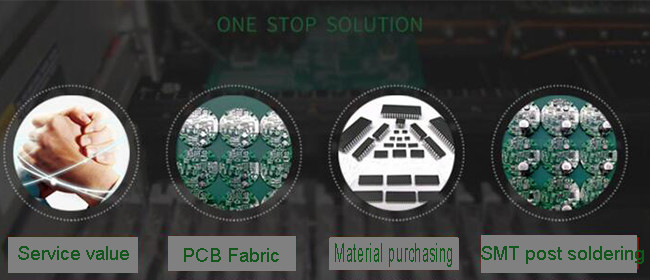
1.Service value
Independent quotation system to quickly serve the market
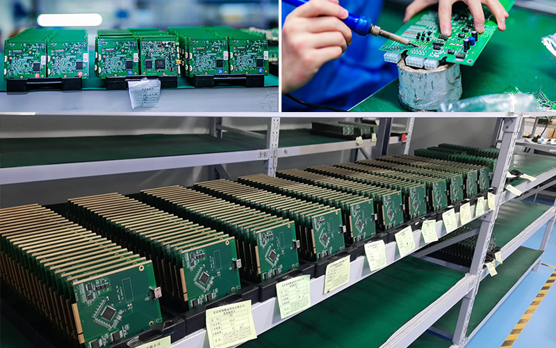
2.PCB manufacturing
High-tech PCB and PCB assembly production line
3.Material purchasing
A team of experienced electronic component procurement engineers
4.SMT post soldering
Dust-free workshop, high-end SMT patch processing
| Product Type | Qty | Normal lead time | Quick-turn lead time |
| SMT+DIP | 1-50 | 1WD-2WD | 8H |
| SMT+DIP | 51-200 | 2WD-3WD | 1.5WD |
| SMT+DIP | 201-2000 | 3WD-4WD | 2WD |
| SMT+DIP | ≥2001 | 4WD-5WD | 3WD |
| PCBA(2-4Layer) | 1-50 | 2.5WD-3.5WD | 1WD |
| PCBA(2-4Layer) | 51-2000 | 5WD-6WD | 2.5WD |
| PCBA(2-4Layer) | ≥2001 | ≥7WD | 5WD |
| PCBA(6-10Layer) | 1-50 | 3WD-4WD | 2.5WD |
| PCBA(6-10Layer) | 51-2000 | 7WD-8WD | 6WD |
| PCBA(10-HDILayer) | 1-50 | 7WD-9WD | 5WD |
| PCBA(10-HDILayer) | 51-2000 | 9WD-11WD | 7WD |
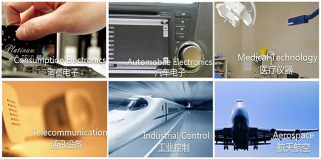
Our products are widely used in the following areas:
1. communication equipment,
2. industrial control,
3.consumer electronics,
4.medical equipment,
5. aerospace,
6.light-emitting diode lighting,
7.automotive electronics etc
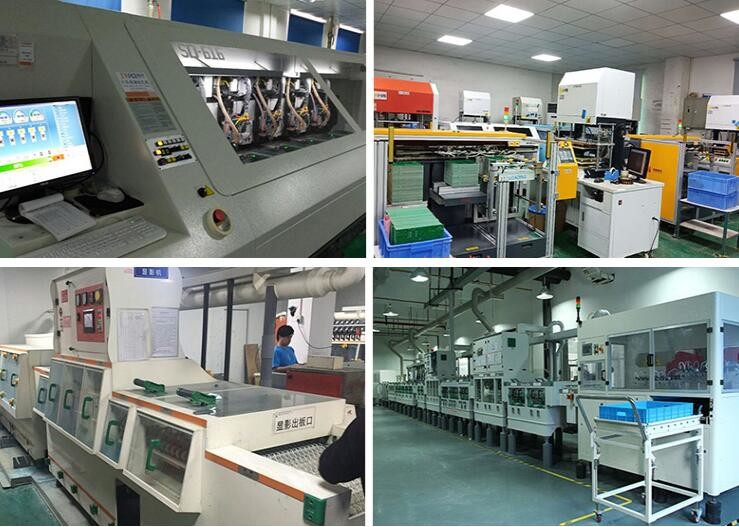
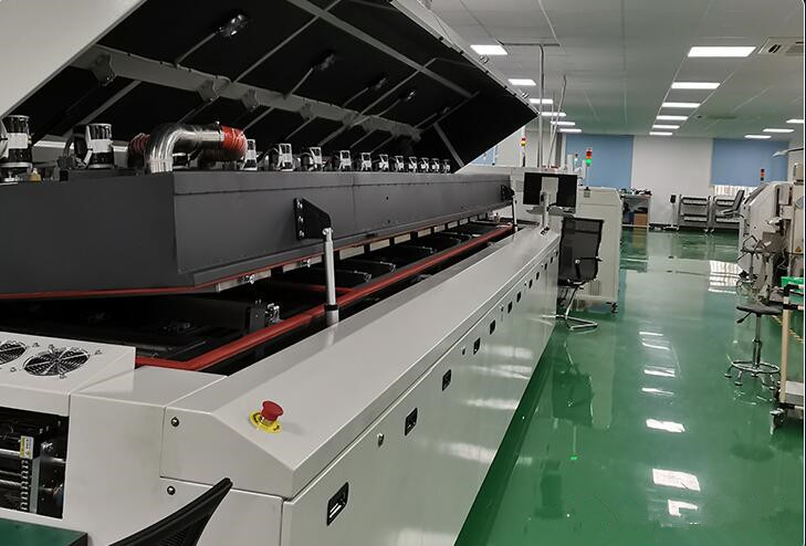
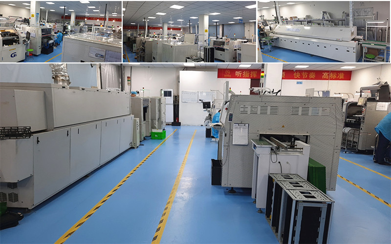
Workshop
1.PCB: Vacuum packaging with carton box
2.PCBA: ESD packaging with carton box
FAQ:
Q1:What service do you have?
A1: We provide turnkey solution including RD, PCB fabrication, SMT,
final assembly,testing and other
value-added service.
Q2:What are the main products of your PCB/PCBA services?
A2:Our PCB/PCBA services are mainly for the industries including
Medical, Automotive, Energy,
Metering/Measurements. Consumer Electronics.
Q3:How can we ensure our information should not let third party to see our design?
A3: We are wiling to sign NDA effect by customer side locallaw and promising to keep customers datain highconfidential level.
Q4:What does Parason need for a customized PCB order?
A4:When you place a PCB order, the customers need to provide Gerber or pcb file.If you do not have the fileinthe correct format, you can send all the details related to the products.
Q5:What will be needed for a customized PCBA order?
A5: When you place a PCBA order, you need to provide Gerber or pcb file and the BOM list to us.
Q6:Do you have an minimum order quantity?
A6:We accept order with as low as a quantity of 1 (piece or panel)
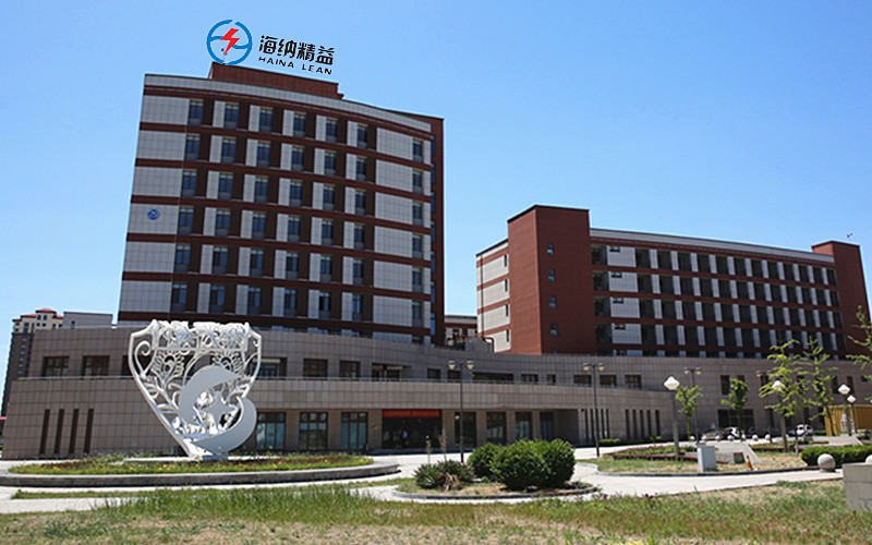
Company information:
Haina Lean Electronics has been turned into a first class manufacture of HDI PCB. We are providing high quality bare PCB,PCB layout design service and PCB assembly service,including components sourcing, function test,conformal coating and complete assembly for clients all.
Our advantages:
1. Our company has passed the ts16949:2009 quality system certification, and the processed products meet the export standards of Europe and America
2. There is no minimum order quantity limit, which supports the whole process from sample to batch.
3. A professional component procurement team, centralized procurement, to save your procurement costs, labor costs, quality costs.
4. Professional sample making: SMT samples will be delivered within 24 hours.
5. Our main customer base: automotive electronics, industrial control, security, communication, power and other high-end.

|
