| Sign In | Join Free | My ecer.jp |
|
| Sign In | Join Free | My ecer.jp |
|
| Categories | Electronics Components |
|---|---|
| Brand Name: | TI |
| Model Number: | SN74LS06N |
| Certification: | Original Factory Pack |
| Place of Origin: | Thailand |
| MOQ: | 10pcs |
| Price: | Negotiation |
| Payment Terms: | Western Union,PayPal,T/T |
| Supply Ability: | 1500PCS |
| Delivery Time: | 1 Day |
| Packaging Details: | please contact me for details |
| FEATURES: | Convert TTL Voltage Levels to MOS Levels |
| FEATURES2: | High Sink-Current Capability |
| FEATURES3: | Input Clamping Diodes Simplify System Design |
| Applications: | Open-Collector Driver for Indicator Lamps and Relays |
| Typical Applications 1: | Inputs Fully Compatible With Most TTL Circuits |
| Package: | DIP-14 |
| Company Info. |
| Anterwell Technology Ltd. |
| View Contact Details |
| Product List |
Small Scale Integrated Circuits SN74LS06N Hex Inverter Open Collector
The SN74LS16 is obsolete and is no longer supplied
Convert TTL Voltage Levels to MOS Levels
High Sink-Current Capability
Input Clamping Diodes Simplify System Design
Open-Collector Driver for Indicator Lamps and Relays
Inputs Fully Compatible With Most TTL Circuits
Description
These hex inverter buffers/drivers feature high-voltage open-collector outputs to interface with high-level circuits (such as MOS), or for driving high-current loads, and also are characterized for use as inverter buffers for driving TTL inputs. The ’LS06 devices have a rated output voltage of 30 V, and the SN74LS16 has a rated output voltage of 15 V.
The maximum sink current for the SN54LS06 is 30 mA, and for the SN74LS06 and SN74LS16 is 40 mA. These devices are compatible with most TTL families. Inputs are diode-clamped to minimize transmission effects, which simplifies design. Typical power dissipation is 175 mW and average propagation delay time is 8 ns.
ORDERING INFORMATION
| TA | PACKAGE† | ORDERABLE PART NUMBER | TOP-SIDE MARKING | |
| 0°C to 70°C | SOIC D | Tube | SN74LS06D | LS06 |
| Tape and reel | SN74LS06DR | |||
| SOP – NS | Tape and reel | SN74LS06NSR | 74LS06 | |
| SSOP – DB | Tape and reel | SN74LS06DBR | LS06 | |
| PDIP – N | Tube | SN74LS06N | SN74LS06N | |
| –55°C to 125°C | CDIP – J | Tube | SN54LS06J | SN54LS06J |
| Tube | SN54LS06J | SN54LS06J | ||
| LCCC – FK | Tube | SNJ54LS06FK | SNJ54LS06FK | |
absolute maximum ratings over operating free-air temperature range (unless otherwise noted)†
Supply voltage, VCC . . . . . . . . . . . . . . . . . . . . . . . . . . . . . . . . . . . . . . . . . . . . . . . . . . . . . . . . . . . . . 7 V
Input voltage, VI (see Note 1) . . . . . . . . . . . . . . . . . . . . . . . . . . . . . . . . . . . . . . . . . . . . . . . . . . . . . . . 5.5 V
Output voltage, VO (see Notes 1 and 2):
SN54LS06, SN74LS06 30 V
SN74LS16 15 V
Package thermal impedance, θJA (see Note 3):
D package 86 °C/W
N package 80°C/W
NS package 76 °C/W Storage
temperature range, Tstg . . . . . . . . . . . . . . . . . . . . . . . . . . . . . . . . . . . . . . . . . . . . . . –65°C to 150°C
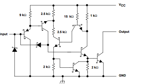
schematic (each gate)

|
