| Sign In | Join Free | My ecer.jp |
|
| Sign In | Join Free | My ecer.jp |
|
| Categories | SiC Substrate |
|---|---|
| Brand Name: | zmsh |
| Model Number: | 2inch-6h |
| Place of Origin: | china |
| MOQ: | 2pcs |
| Price: | 200usd/pcs by FOB |
| Supply Ability: | 1000pcs |
| Delivery Time: | within 15days |
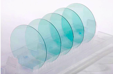
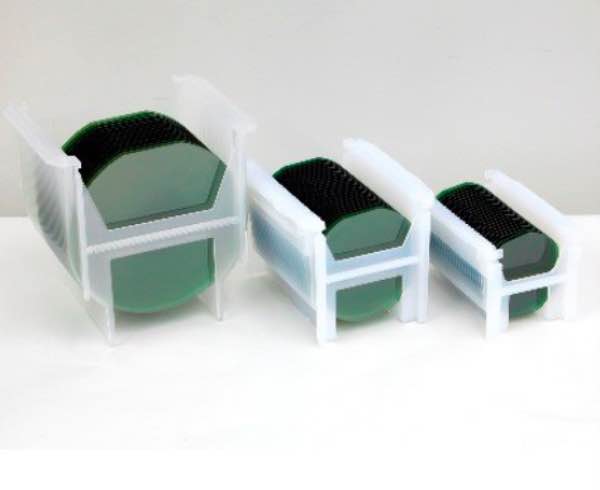
| Packaging Details: | in cassettes of single wafer containers |
| material: | sic single crystal |
| industry: | semiconductor wafer, |
| applications: | device,epi-ready wafer, 5G,power electronics,detector, |
| color: | green,blue,white |
| customized: | ok |
| type: | 6H-N |
| Company Info. |
| SHANGHAI FAMOUS TRADE CO.,LTD |
| Verified Supplier |
| View Contact Details |
| Product List |
2inch 6H-Semi sic wafer ,customized sic substrates , 2inch 6H-N sic wafers , sic crystal ingots ,Silicon Carbide Wafer
This 2-inch 6H semi-insulating silicon carbide (SiC) wafer is designed for applications requiring low power consumption, particularly in detectors. Silicon carbide is known for its exceptional high-temperature stability, high breakdown voltage, and excellent thermal conductivity, making it an ideal material for high-performance electronic devices and sensors. The wafer's superior electrical insulation properties and low power consumption significantly enhance detector efficiency and lifespan. As a key component for achieving low-power, high-performance detection technology, this SiC wafer is well-suited for various demanding applications.
Application areas
SILICON CARBIDE MATERIAL PROPERTIES
| Property | 4H-SiC, Single Crystal | 6H-SiC, Single Crystal |
| Lattice Parameters | a=3.076 Å c=10.053 Å | a=3.073 Å c=15.117 Å |
| Stacking Sequence | ABCB | ABCACB |
| Mohs Hardness | ≈9.2 | ≈9.2 |
| Density | 3.21 g/cm3 | 3.21 g/cm3 |
| Therm. Expansion Coefficient | 4-5×10⁻⁶/K | 4-5×10⁻⁶/K |
| Refraction Index @750nm | no = 2.61 ne = 2.66 | no = 2.60 ne = 2.65 |
| Dielectric Constant | c~9.66 | c~9.66 |
| Thermal Conductivity (N-type, 0.02 ohm.cm) | a~4.2 W/cm·K@298K c~3.7 W/cm·K@298K | |
| Thermal Conductivity (Semi-insulating) | a~4.9 W/cm·K@298K c~3.9 W/cm·K@298K | a~4.6 W/cm·K@298K c~3.2 W/cm·K@298K |
| Band-gap | 3.23 eV | 3.02 eV |
| Break-Down Electrical Field | 3-5×10⁶V/cm | 3-5×10⁶V/cm |
| Saturation Drift Velocity | 2.0×10⁵m/s | 2.0×10⁵m/s |
Standard spec.
| 2inch diameter Silicon Carbide (SiC) Substrate Specification | ||||||||||
| Grade | Zero MPD Grade | Production Grade | Research Grade | Dummy Grade | ||||||
| Diameter | 50.8 mm±0.2mm | |||||||||
| Thickness | 330 μm±25μm or 430±25um | |||||||||
| Wafer Orientation | Off axis : 4.0° toward <1120> ±0.5° for 4H-N/4H-SI On axis : <0001>±0.5° for 6H-N/6H-SI/4H-N/4H-SI | |||||||||
| Micropipe Density | ≤0 cm-2 | ≤5 cm-2 | ≤15 cm-2 | ≤100 cm-2 | ||||||
| Resistivity | 4H-N | 0.015~0.028 Ω•cm | ||||||||
| 6H-N | 0.02~0.1 Ω•cm | |||||||||
| 4/6H-SI | ≥1E5 Ω·cm | |||||||||
| Primary Flat | {10-10}±5.0° | |||||||||
| Primary Flat Length | 18.5 mm±2.0 mm | |||||||||
| Secondary Flat Length | 10.0mm±2.0 mm | |||||||||
| Secondary Flat Orientation | Silicon face up: 90° CW. from Prime flat ±5.0° | |||||||||
| Edge exclusion | 1 mm | |||||||||
| TTV/Bow /Warp | ≤10μm /≤10μm /≤15μm | |||||||||
| Roughness | Polish Ra≤1 nm | |||||||||
| CMP Ra≤0.5 nm | ||||||||||
| Cracks by high intensity light | None | 1 allowed, ≤2 mm | Cumulative length ≤ 10mm, single length≤2mm | |||||||
| Hex Plates by high intensity light | Cumulative area ≤1% | Cumulative area ≤1% | Cumulative area ≤3% | |||||||
| Polytype Areas by high intensity light | None | Cumulative area ≤2% | Cumulative area ≤5% | |||||||
| Scratches by high intensity light | 3 scratches to 1×wafer diameter cumulative length | 5 scratches to 1×wafer diameter cumulative length | 5 scratches to 1×wafer diameter cumulative length | |||||||
| edge chip | None | 3 allowed, ≤0.5 mm each | 5 allowed, ≤1 mm each | |||||||
ZMKJ can provides high quality single crystal SiC wafer ( Silicon Carbide ) to electronic and optoelectronic industry . SiC wafer is a next generation semiconductor material , with unique electrical properties and excellent thermal properties , compared to silicon wafer and GaAs wafer , SiC wafer is more suitable for high temperature and high power device application . SiC wafer can be supplied in diameter 2-6 inch , both 4H and 6H SiC , N-type , Nitrogen doped , and semi-insulating type available . Please contact us for more product information .

Packing and Delivery
>Packaging – Logistcs
we concerns each details of the package , cleaning, anti-static ,
shock treatment .
According to the quantity and shape of the product , we will take a different packaging process! Almost by single wafer cassettes or 25pcs cassette in 100 grade cleaning room.

|
