| Sign In | Join Free | My ecer.jp |
|
| Sign In | Join Free | My ecer.jp |
|
| Categories | Sapphire Wafer |
|---|---|
| Brand Name: | zmsh |
| Model Number: | A-plane 2INCH |
| Place of Origin: | china |
| MOQ: | 25pcs |
| Price: | by case |
| Supply Ability: | 1000pcs/months |
| Delivery Time: | 15-20days |
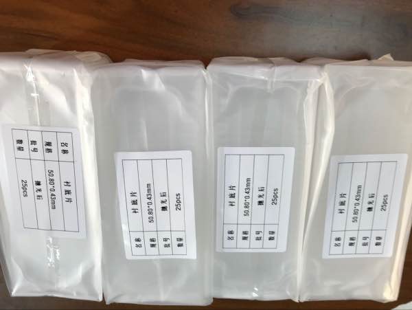
| Packaging Details: | Vacuum-sealed containers with nitrogen backfill in a class 100 environment |
| material: | 99.999% Al2O3 |
| industry: | led,optical glass,epi-ready wafer |
| application: | semicondutor wafer, led chip, optical glass window, electronic ceramics |
| color: | white or red or blue |
| vision light transmissivity: | 85% |
| advantagement: | high hardness9.0,wear resistance, |
| type: | 2inch A-axis |
| Thickness: | 0.43mm |
| Company Info. |
| SHANGHAI FAMOUS TRADE CO.,LTD |
| Verified Supplier |
| View Contact Details |
| Product List |
Sapphire Indtroduce
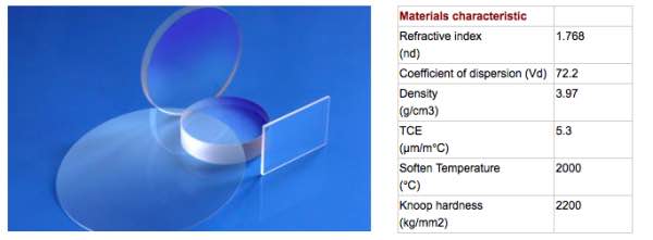
| Product Name: | Aluminum oxide (Al2O3) crystal substrate Sapphire crystal | ||||||||||||||||||||||
| Product Description: | Al2O3 single crystal (Sapphire, also known as white stones, sapphire) has good thermal properties, excellent electrical characteristics and dielectric properties, and anti-chemicalcorrosion, it is high temperature, thermal conductivity, high hardness, infrared transparent, chemically stable good. Widely used in high-temperature infrared window materials and III-V nitride epitaxial film substrate and a variety of materials to meet the growing blue, purple, white light-emitting diode (LED) and blue laser (LD) needs, Branch Crystal company specializing in the production of high quality polished sapphire crystal and epitaxial substrates will provide you with a lot of high quality and low price monocrystalline substrate. | ||||||||||||||||||||||
| Technical parameters: |
| ||||||||||||||||||||||
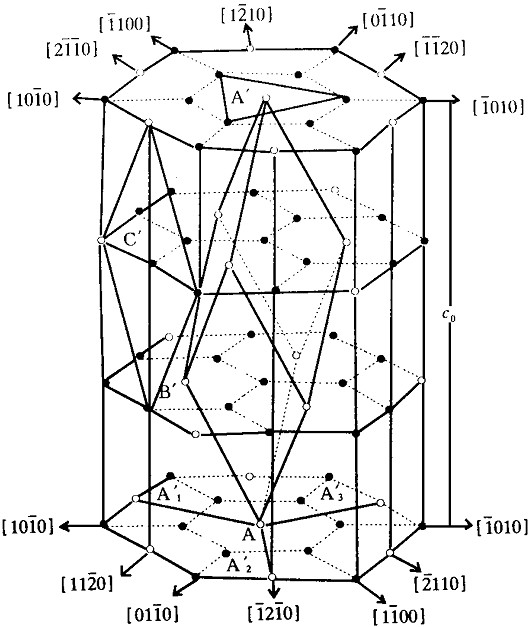
| Specifications: | C, A, M, R Tolerance: + / -0.2 degrees dia2"~dia dia15" x 250mm Single throw or double throw, Ra <5A Note: according to customers' requirements and size of the corresponding direction. | ||||||||||||||||||||||
| Standard Packaging: | 1000 clean room, 100 clean bag or single box packaging |
Diameter:50.8.±0.2mm
Thickness :430±15um or 330±15um
Primary flat:16±1mm
OF Orientation flat: OFF C axis±0.1° C-plane(0001)
Frontside Surface Roughness:Ra<0.2nm
Backside Surface Roughness: 0.8~1.2um
( Or double side polished, both side Ra<0.2nm)
TTV:<10um
BOW:-10~0um
WARP:<10um
Laser Mark Series No. by needs
Package:Vacuum-sealed containers with nitrogen backfill in a class 100 environment
Cleanliness :Free visible contamination
If needing, 3-6inch A-axis wafers also can be provided.
Sapphire Application
Application
- For LED substrate application
Hostile environment
Optical transmission from ultraviolet to near infrared
High temperature and ultra low temperatures
Radiation resistance
Sapphire wafer and substrate applications include:
- Microelectronic IC applications - SOS Silicon-on-Sapphire
- Growth of superconducting compounds / Gallium Nitride - Infrared
detectors
- Hybrid microelectronics - Polishing carriers
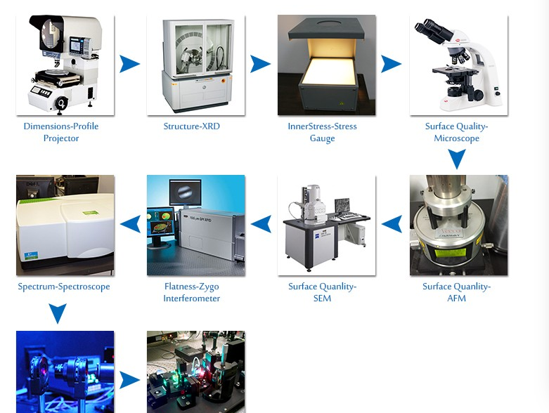
QC flow of sapphire wafer produce
FAQ:
1. Q: What's the delivery time?
A: (1) For the standard products
For inventory: the delivery is 5 workdays after you place the order.
omized products: the delivery is 2 -4 weeks after you order contact.
2. Q: What's the way of shipping and cost?
A:(1) We accept DHL, Fedex, EMS etc by FOB.
3. Q: How to pay?
A: T/T, Paypal, Secure payment and Assurance payment.
4. Q: What's your MOQ?
A: (1) For inventory, the MOQ is 25pcs. if 50pcs it's better.
(2) For customized products, the MOQ is 25pcs up.
5. Q: Do you have standard products?
A: Our standard products in stock. as like 2inch 0.43mm 1sp or 2sp thickness each orientation in stock.
>>Packaging – Logistcs
Worldhawk concerns each details of the package , cleaning,
anti-static , shock treatment . According to the quantity and shape
of the product , we will take a different packaging process!

|
